コンピューティング
中国、予想よりはるかに早くEUVをマスター

 Securities.io を Google の優先ソースに追加
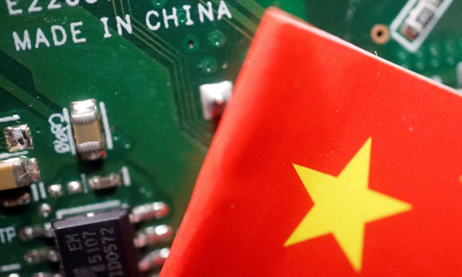
中国のEUVプロトタイプが早期に登場
As computing techniques improved, more and more advanced chips were invented. The latest generation of 3nm and 2nm nodes is so small that the normal light wavelength is simply too large to reliably pattern features at this scale.
これは新しいことではなく、業界は長年にわたりDUV(Deep UltraViolet)光を用いてシリコンウェーハのリソグラフィを行ってきました。しかし、最先端チップ設計のナノスケールに到達するためには、さらに短波長の光源が必要でした。
この光源とリソグラフィ手法はEUV(Extreme UltraViolet)と呼ばれます。

出典: Zeiss
これまで、EUVはオランダの企業ASML(ASML )が独占しており、世界で唯一のEUVリソグラフィ装置メーカーでした。
2019年、TSMCの7nmノードチップは初のEUVプロセスで製造され、市場に大量供給されました。
EUV技術へのアクセス管理は、米国が中国の半導体産業に対して課した制裁の中心的要素です。2018年にさかのぼり、米国はオランダに対しASMLがEUV装置や関連部品、保守サービスを中国に販売することを阻止するよう圧力をかけました。
この考え方は、EUVへのアクセスを制限すれば中国の先端チップ製造能力が鈍化し、先進的AIアクセラレータの輸出制限と合わせて米国がAI競争で優位を保てるというものでした。
しかし、現在では中国の半導体自立への取り組みが圧力下で加速しているようで、ロイターが中国がEUVプロトタイプ装置を完成させたと報じています。開発が順調に進めば、2028年頃からチップ生産が開始でき、そこから生産規模を拡大できる可能性があります。
Not only could this complicate Western efforts to constrain China’s access to leading-edge manufacturing, but it may also represent a long-term threat to the Western-centric semiconductor supply chain—arriving years sooner than even many China‑optimistic analysts expected.
「4月、ASML CEOのChristophe Fouquetは、中国がこの技術を開発するには『何年も、何年も』かかるだろうと述べました。」
「しかし、ロイターが初めて報じたこのプロトタイプの存在は、中国が半導体自立に向けてアナリストが予想したよりも数年早く到達している可能性を示唆しています。」
中国の予想外のEUV突破はASMLの独占を揺るがし、西側制裁戦略を弱体化させ、世界的な半導体勢力図に長期的な変化をもたらす可能性があります。
EUVリソグラフィが実際にどのように機能するか
What makes EUV so unique—and why it remained an ASML monopoly for many years—is that EUV is not just one technology, but the assembly of many feats of ultra‑precise engineering into a single integrated system.

最初の部分は約30kWの超強力CO2レーザーで、世界で最も強力なパルス産業用レーザーの一つです。ASMLの装置では、ドイツ企業Trumpfが製造しています。
しかし、このレーザー自体がEUV光を生成するわけではなく、エネルギー源です。EUVを生成するために、システムは微小な溶融スズの滴をプラズマに過熱し、ASML装置は1秒間に約50,000滴のスズを発射します。
プラズマは極めて高温(しばしば約220,000°C(360,000°F))に加熱され、太陽表面よりもはるかに高温の条件を作り出し、産業工学の限界に挑みます。
この全プロセスはほぼ完全な真空中で行われなければなりません。空気(および多くの材料)はEUV光を吸収してしまうためです。

出典: SemiEngineering
そして、まだ終わりではありません。生成されたEUV光は、シリコンウェーハに最先端のパターンを描くために、驚異的な精度で指向、整形、焦点合わせが必要です。トランジスタ密度が100億個/mm²に近づく先端ノードでは、これが不可欠です。
These curved mirrors, developed by the German optics leader Zeiss, must be manufactured and aligned with accuracy approaching the atomic level.
「もしこのEUVミラーをドイツ全土に拡大したとしたら、最大の凹凸—いわばツークシュピッツェ—は0.1ミリメートルの高さになるでしょう。」
この精度は極端で、ミラーの指向精度はしばしば鮮やかな例えで語られます。例えば、EUVミラーで月へビームを向けた場合、月面にあるピンポン球サイズの目標に命中できるほどの精度が理論上求められます。
These optics are also coated with a multilayer stack—often alternating materials like silicon and molybdenum—only a few atoms thick per layer.
「ここでは最大100層が重ねられています。単層は光の約1%しか反射せず、損失が大きすぎます。
結果として、光の約70%が有効に反射されます。」
Finally, the silicon wafer itself must move and align with extraordinary precision. Sensors measure positioning continuously, and the wafer stage must maintain accuracy while resisting deformation from thermal change and high‑speed motion.
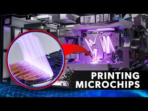
So, when taking into consideration all of these steps (and the explanation above is still an oversimplification), it becomes clear why replicating EUV is so difficult: it requires reproducing not only a design, but a vast ecosystem of materials, metrology, controls, optics, vacuum systems, and ultra‑clean manufacturing—integrated into one machine.
なぜEUVは再現が極めて困難なのか
Swipe to scroll →
| サブシステム | サプライヤー支配力 | 難しさの理由 |
|---|---|---|
| EUV光源(スズプラズマ) | ASMLエコシステム + Trumpf | 高出力レーザー、滴のタイミング、プラズマ安定性、デブリ除去 |
| 投影光学系 | Zeissほぼ独占 | 原子レベルの表面完璧性、マルチレイヤコーティング、スケールでの歩留まり |
| 真空システム | 複数の専門サプライヤー | 移動ステージと高熱負荷を伴う超クリーンな真空保持 |
| 計測・センサー | 高度に専門化されたグローバルチェーン | リアルタイムのナノメートルフィードバックループ;較正、ドリフト、汚染管理 |
| 制御ソフトウェア | ASML独自 | 数千のサブシステムにわたる緊密な統合;プロセスノウハウ |
| ウェーハステージ&メカニクス | 精密メカトロニクスリーダー | 振動なしの極端な加速;熱安定性;スケールでの再現性 |
中国のEUV「マンハッタン・プロジェクト」:総合的な半導体動員
総合的な動員
Considering how crucial leading‑edge chips are for competition in AI, advanced robotics, and military technology, comparing China’s domestic EUV push to a Manhattan Project is not mere rhetoric—it reflects the scale and urgency of the effort.
まず、公共・民間の巨額資本が半導体全体への取り組みに投入されたと見られ、2025年初頭に少なくとも370億ユーロが動員されたと報じられています。大学研究、産業施設、重要サプライヤーへの補助金、保証購入、国家主導の将来チップ需要など、さらに多くが投入されたと考えられます。
そして、2022年12月にHuaweiがEUV関連特許を出願したことが報じられましたことは、驚きではありません。
同時に、別の中国企業SMICは古いDUV装置を用いてEUVなしで5nmクラスのチップを製造したと報じられています—制約されたツールで「やりくり」するインセンティブの強さを示しています。
さらに別の概念として、粒子加速器(シンクロトロン)でEUV光を生成するという方向性が2023年にすでに議論され、2022年の科学論文にも結び付いています。
これらすべての取り組みは、中国の機関や企業がEUVをマスターするか、あるいはEUVなしで競争力のある代替手段を構築することに、いかに巨大な重要性を置いているかを示しています。
Central to these efforts has been Huawei, the heavily sanctioned Chinese tech giant.
「Huaweiは国内のオフィス、製造工場、研究センターに従業員を配置し、プロジェクトを推進しています。」
「半導体チームに配属された従業員は現場で寝泊まりし、勤務週中は自宅へ帰れず、機密性の高いタスクを担当するチームは電話使用が制限されています。」
人材獲得が中国のEUVプログラムを加速させた方法
Another effort to unlock EUV—more secretive—has reportedly focused on acquiring the experience and human talent that made EUV possible in the first place.
Top engineers, including some who had worked at ASML and later retired, were prime targets for recruitment. Reports also suggest that other current employees of ASML have been approached for recruitment as far back as 2020.
「ASMLからリクルートされた中国人ベテラン技術者は、署名ボーナスと引き換えに偽名で発行された身分証明書を受け取ったと関係者が語っています。」
These recruitments were reportedly part of a broader effort to bring top talent into China, with semiconductor experts working abroad being offered signing bonuses and subsidies years ago.
Bending some national rules to make it more convenient for these hired experts also appears to have occurred in isolated cases. For example, some naturalized citizens of other countries were reportedly given Chinese passports and allowed to maintain dual citizenship, despite China officially prohibiting dual citizenship.
The fact that many of these engineers are of Chinese nationality or origin may also have made recruitment easier.
Overall, claims that China “only steals technologies” are often an oversimplification of a fast‑growing research and engineering ecosystem. Still, in this specific case, the overlap with ASML trade secrets could be meaningful.
「ASMLは元従業員の就業先を制御できませんが、全従業員は契約上の機密保持条項に拘束されており、同社は『営業秘密の窃盗に対し法的措置を成功裏に取った』と述べました。」
中国初のEUVリソグラフィプロトタイプの内部
The result of hiring ex‑ASML employees, reverse‑engineering EUV parts, and independent development of domestic alternatives appears to have produced a prototype that is significantly larger than ASML’s typical 180‑ton, school‑bus‑sized EUV systems—reportedly taking up an entire factory floor.
This could indicate the prototype is either more power‑hungry, less compact, less efficient, or simply at an earlier stage of optimization than ASML’s production designs.
Salvaged components from older ASML machines, along with secondhand markets for parts from ASML suppliers, could also have helped assemble a working prototype while domestic manufacturing ramps or quality improves.
A key component that may still be missing—and exceptionally difficult to replicate at comparable performance—is Zeiss optics. This is reportedly one reason the machine cannot yet produce chips at the desired level.
High‑NA EUV:チップ軍拡競争の次なるフロンティア
If EUV took ASML decades to develop, the emergence of a Chinese prototype suggests that catching up—at least in basic system demonstration—could happen much faster than many assumed.
This puts pressure on Western semiconductor leaders to push harder into the next generation: High‑NA (Numerical Aperture) EUV.
High‑NA EUV is already being tested by companies like Intel (INTC ), and it has been evaluated by Samsung and TSMC. Intel has publicly targeted production volume timelines around 2028, while both TSMC and Samsung appear more cautious, reserving High‑NA EUV for future <2nm nodes rather than rushing it into mass deployment.
「光学系が光を受け取る角度が大きくなるほど、表示されるディテールは細かくなります。つまり、光学EUVシステムはどんどん大きくなっていくということです。」
High‑NA systems use even larger optical elements, which may provide a durable edge to ASML via its optics partner Zeiss.

出典: Zeiss
A mirror for High‑NA EUV lithography is about twice as large and ten times as heavy as current EUV mirrors—making the total system even larger, heavier, and more complex.
「High‑NA‑EUVリソグラフィ用投影光学部品は40,000以上あり、総重量は約12トンに達し、従来のEUVリソグラフィの7倍の体積と重量になります。」
投資家にとって何を意味するか?
In the short term, this likely changes little. China’s EUV machine is reportedly only a prototype, and it remains unclear how much of it relies on repurposed or salvaged ASML parts versus purely China-made components.
しかし、中国が永遠に失敗し続けると想定するのは難しいです。十分な専門家、資金、時間があれば、EUVの能力の大部分を最終的に再現できない理由はありません—特に部品、材料、計測のエコシステムが成熟すればなおさらです。
Zeissミラーなど特定の部品を中国が置き換えられないという懐疑論も慎重に扱うべきです。以前の分析では中国は15年以上遅れているとされていましたが、現在はプロトタイプが報告されています。
長期的には(5〜10年)、中国はファウンドリレベルだけでなく、装置製造レベルでも独立した半導体サプライチェーンを構築できる可能性があります。
当初は、先進的な国内生産は国内需要を優先し、中国への先端チップ、製造装置、関連部品の販売が減少するでしょう。
時間が経つにつれて、これは西側半導体装置メーカーやサプライヤーの売上高と利益率に圧力をかけ、以前のR&D投資レベルを維持する能力を低下させる可能性があります。
More concerning for companies like ASML and other equipment makers—and even for foundries—China-made advanced chips could eventually compete directly in external markets, especially across expanding BRICS and SCO (Shanghai Cooperation Organization) commercial networks.
ASMLとTSMCが短期的には支配的であり続ける一方で、中国のEUV進展は長期的な競争圧力をもたらし、装置、ファウンドリ、チップ市場を再構築する可能性があります。
結論
The appearance of a Chinese EUV prototype years earlier than many expected is a genuine milestone. It suggests that export controls and sanctions are unlikely to permanently cap technological capability in a sector where the West has long held a structural advantage.
At best, restrictions may delay progress; at worst, they can accelerate it by creating a protected domestic market of roughly 1.5 billion people with strong state support and industrial capacity.
This does not mean China will immediately begin producing leading‑edge chips on domestic EUV tools. But it does mean the trajectory toward that goal is now clearer—and likely faster—than many previously assumed.
Overall, it reinforces that China is evolving into a major tech power, not merely the world’s largest manufacturing base.
While China’s breakthrough changes the long‑term horizon, investors looking for immediate dominance in the semiconductor space must still look to the current market leader.
半導体企業 – TSMC
TSM 価格チャート
中国がテック大国として台頭することは戦略的に重要ですが、現時点では中国の半導体製造装置は依然として西側の最先端システムに遅れを取っているか、あるいはそこに迫りつつある段階です。
したがって、ファウンドリ事業においては、プロセスの規律、歩留まりの学習、運用経験が今後の10年で決定的な要因となるでしょう。
最終的に、半導体生産はニッチな専門知識と規模の経済による大量生産能力に支配されます。このモデルを最も熟達しているのは、超先端チップ製造で台湾のリーダーであるTSMCです。
TSMCは主にシリコンチップを製造しており、最も強力な3nmノードと今後の2nmクラスノードを手掛けています。そして、最も先端(かつ最も高価)なチップを製造しているため、世界のファウンドリ収益の支配的シェアを占めています。

出典: Eric Flaningam
TSMCは米国でも製造能力を拡大しており、特にアリゾナ工場への大規模投資を通じて進めています。
High‑NA EUVの開発がすでに進行中であることから、TSMCはSMICなどの中国競合に対して、歩留まり、信頼性、大量生産の成熟度で数年先んじた状態を維持できるでしょう。
And even as it has competed fiercely against Samsung, Intel, and other foundries, TSMC is still positioned to defend its lead against rising China‑based competition—at least for the foreseeable future.
最新のTSMC(TSM)株式ニュースと動向