Informatique
ASML (ASML) : la pierre angulaire des semi-conducteurs modernes

Les outils de la fabrication de puces
Semiconductors, and especially computer chips, have quickly become one of the world’s most important technologies and commodities on Earth. From the early days of the PC era to the rise of smartphone & cloud computing, and AI, the importance of chips and demand for them has only grown.

Source: Applied Materials
C’est une industrie intéressante, où aucun acteur n’est intégré verticalement ; à la place, elle est constituée d’une constellation d’entreprises ultra‑spécialisées, chacune réalisant l’une des nombreuses étapes critiques pour transformer le sable ordinaire (silicium) en machines pensantes.
Les plus grandes entreprises du secteur sont soit des concepteurs de puces comme Nvidia (NVDA ), soit des « fondeurs » qui fabriquent réellement les puces comme TSMC (TSM ) (suivez le lien pour des rapports d’investissement dédiés sur ces entreprises).
Ces entreprises dépendent fortement de fournisseurs spécialisés pour les machines nécessaires à la production des puces.

Source: ASML
Et aucune n’est plus importante que l’entreprise qui détient le monopole de la lithographie EUV (Extreme UltraViolet), la néerlandaise ASML.
(ASML )
Le rôle d’ASML dans la fabrication de semi-conducteurs
Comment la lithographie alimente la miniaturisation des puces
ASML is a specialist in lithography machines. Lithography (literally meaning “rock engraving) is how the “node” of a processor gets engraved on a silicon wafer, turning it into a computer chip.

Source: Nature
Plus la puce est avancée, plus le nœud est petit et plus le processus de lithographie est complexe. La miniaturisation continue des nœuds et l’amélioration de la lithographie ont permis aux ordinateurs de devenir chaque année plus puissants, suivant la loi de Moore.

Source: Steven Jurvetson
La lithographie est une étape du processus complet qui transforme une tranche de silicium en puces informatiques, avec généralement 40 à 80 cycles pour fabriquer une puce complète.

Source: ASML
Une limite physique clé de la lithographie est que le nœud gravé ne peut pas être plus grand que la longueur d’onde de la lumière puissante utilisée pour le faire.

Source: ASML
Ainsi, à mesure que les transistors deviennent plus petits, une fréquence de lumière de plus en plus élevée est requise, aujourd’hui se situant de plus en plus dans l’extrémité supérieure du spectre ultraviolet.
The first step of leaving the visible light spectrum was with I-line, followed soon by DUV (Deep Ultraviolet) lithography.

Source: Icometrue
These methods were the ones carrying the industry during the era of ever more performing smartphones and data centers. But for the most advanced tools, a new technology was needed: EUV (Extreme Ultraviolet) lithography.
Qu’est-ce que la lithographie EUV et comment fonctionne-t-elle ?
EUV allows for ultra-small nodes, up to 7nm, or even 5nm, 3nm, and beyond. These advanced node levels are often considered necessary for applications like AI, machine learning, 5G, AR/VR, and advanced cloud services.
While ASML is a leader in DUV technology, EUV is even more important, as the company is the sole manufacturer of EUV chip-making machinery, although some Chinese companies are looking to enter the sector as soon as possible (see below for more on that topic).
EUV technology is extremely difficult to master, due to a series of technical limitations:
- The process takes place in a vacuum environment because nearly everything absorbs EUV light.
- It requires a very strong energy source, in the form of a powerful laser, with up to 40kW laser being used. This sort of laser amplifier requires 7.3 kilometers of cable, weighs 17 tons, and contains 450,000+ parts.
- The laser excites tiny droplets of tin 25 microns in diameter, with 50,000 droplets falling per second.
- The tin is then vaporized into a plasma by the laser, emitting EUV light.

Source: Semi Engineering
Each of these steps requires extremely advanced measurement, tools, controls, and sensors, all engineering at a precision quality measured in micrometers and nanoseconds.
Through deep expertise built during decades of building lithography machines, ASML is the (so far?) uncontested master of EUV technology. It has also built a dense network of key suppliers, with, for example, mirrors up to 1 meter across, with surface smoothness down to picometers (one trillionth of a meter).
Besides very precise machines, EUV also requires specialized and proprietary software for calibration, diagnostics, evaluation, and automation.
While EUV is certainly the future of the company, and a large part of its revenues, less advanced DUV-made chips still represent the bulk of the world’s semiconductor production.

Source: ASML
ASML
Aperçu de l’entreprise ASML & indicateurs clés
The company was founded in 1984 as a joint venture between the Dutch companies ASM and Philips. It currently employs 44,000+ people in 60 locations. The company has been collaborating with TSMC from inception, and was already supplying lithography for 90nm nodes in 2004.
By 2011, it had provided lithography machines for 32nm nodes, with an average lithography machine costing €27 million at the time.
By 2022, it had sold 140 EUV machines, each costing $200M+, requiring three Boeing 747s to transport one of the 180-ton machines.
Indicateurs ASML
In 2024, ASML made €28.3B in revenues from selling 583 lithography machines. The company enjoys remarkable 51.3% gross margins, allowing it to easily reinvest €4.3B in R&D, almost double compared to 2020 levels.

Source: ASML
The company expects revenues to grow to €44B-€60B by 2030, with gross margin at 56-60%.
ASML’s industry-leading success in lithography has been rewarded with massive returns for its shareholders. €3B were returned to shareholders in 2024, and dividends have tripled since 2018.

Source: ASML
The company massively outperformed the overall Nasdaq in the past 15 years, even in a decade very favorable to tech stocks in general, and in line with the overall semiconductor indexes.

Source: ASML
The company expects the installed base of lithography machines to keep growing into 2030, strongly driving increasing revenues from maintenance and service upgrades.

Source: ASML
EUVs are not the most sold machines per unit, but represent half of the company’s revenues due to the higher price tag.
Most of the sales at the end of 2024 and early 2025 went to Taiwan, South Korea, the USA, and China. In general, sales in Taiwan can be assumed to be mostly directed to TSMC, in South Korea to Samsung, and in the USA to TSMC (opening a new foundry in Nevada) and to Intel (INTC ).

Source: ASML
Sales to China used to be a lot larger, but sanctions against China by the USA and Chinese chip makers trying to switch to local suppliers have reduced ASML sales to the country to only older lithography technologies.
Risques du marché chinois d’ASML & impact des sanctions
Guerres de sanctions
As China is, together with Taiwan, one of the world’s largest semiconductor producers in the world, ASML used to enjoy a lot of sales in this market.
However, many years of escalating tensions and increasingly punitive sanctions against the Chinese semiconductor industry by successive US administrations have drastically changed this market for ASML.
In the summer of 2022, the USA banned the export of EUV machines to China. This was possible because while ASML is a Dutch company, it relies on key American IP for the production of its lithography machines.
Later on, even exports of DUV machines like ASML’s TWINSCAN NXT:1980Di were restricted, giving China only access to less advanced DUV technology. This sanction round was in part due to the recent success of Huawei in producing advanced chips without EUV machines in septembre 2023.
Solutions chinoises
Huawei is aiming to develop its own EUV solutions, with a patent already deposited in décembre 2022.
Another Chinese company, SMIC, has managed to use older DUV machines to produce 5nm chips without EUV.
“This involved stacking multiple lithography and etching steps, specifically using SAQP, to mimic the precision of EUV. The method is slower, more error-prone, and expensive, but it works.”
Both SMIC and Huawei are looking at creating 3nm chips as well, using self-aligned quadruple patterning (SAQP) lithography. Huawei is also working on a 3nm chip design that replaces silicon with carbon nanotubes.
Lastly, China-made EUV machines could also come to the market soon, at first for domestic use. Another alternative could be to generate the EUV light not with tin plasma, but a particle accelerator, an idea already discussed in 2023, based on a scientific publication from 2022.
Un risque pour ASML ?
Overall, it is likely that the Chinese market will be lost for ASML in the long run, with the country unable to rely on Western technology and having to rebuild from scratch an entire parallel semiconductor supply chain.
This is, for now, mostly a question of strategic rivalry between the USA and China, more than a business threat to ASML.
This is because of a few reasons:
- The sales of DUV to China are just a fraction of ASML’s total revenues.
- The methods bypassing EUV with older DUV are technically feasible, but less reliable and therefore result in more expensive chips.
- This makes them viable for Huawei and other Chinese electronics companies locked out of advanced chips, but not economically competitive in international markets.
- Huawei-made EUV machines will need a lot of improvement and fine-tuning, and will be produced in a limited number, only able to satisfy Chinese domestic demand for many years.
- A cyclotron-based EUV generation is still very theoretical and will take years or even decades to become a viable alternative to the currently used EUV technology.
Ventes non-EUV
Unconnected to the question of Chinese attempts at developing EUV machines, DUV sales are likely to stay stable. This is because while EUV has become the standard for most LOGIC and DRAM critical layers, all other layers are patterned using DUV technology.
So the strong position of ASML in DUV guarantees stable revenues, including servicing and maintenance of the existing parks, with each machine operating for 20+ years.
This makes the development and adoption of EUV important, but not vital to the company’s short-term perspectives.
The same can be said for annex systems to lithography machines, like sensors and metrology (measurements) of the finished product for quality control.

Source: ASML
| Technology | Node Size | Typical Use | Key Limitation |
|---|---|---|---|
| DUV | 14nm–90nm+ | Puces plus anciennes, couches non critiques | Pas adapté aux nœuds les plus petits |
| EUV | 7nm–3nm | Logique avancée, DRAM | Complexe, coûteux, haute énergie |
| High-NA EUV | 2nm and smaller | Puces haute performance de prochaine génération | Coût plus élevé, déploiement limité |
Avenir de la lithographie
ASML keeps innovating and is also actively doing acquisitions of new key technologies, like the optical glass maker Berliner Glas Group in 2020, allowing it to push for the next generation of chip-making machines.

Source: ASML
Chinese competitors might come with commercial-scale EUV solutions in the coming years. But ASML is already working on the next step, called high-NA lithography. The “NA” refers to numerical aperture, a measure of how much light an optical system can gather and focus.
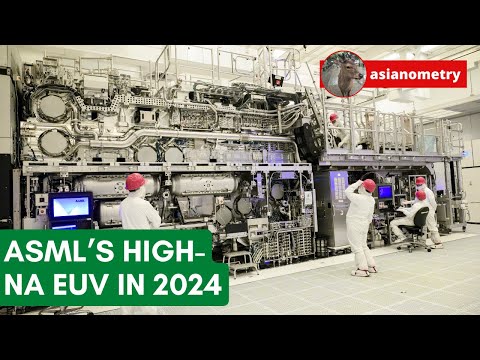
ASML is progressing quickly on this technology: its latest optics innovation sets the base for its EUV roadmap toward picometer stability (1/200 Si atom) on aspheric mirrors.
High-NA EUV optics should help create a higher productivity EUV platform. By doing so, it could push the improvements of EUV performance and productivity far into the next decade (>2030).

Source: ASML
High-NA technology should not only be more precise and quick, it should also be more energy efficient, a growing concern as increasingly powerful lithography machines now come with significant energy bills to operate.
Most likely, high-NA EUV will be the method used for mass production of 2nm node chips and smaller.

Source: ASML
Intel has been an early adopter of High-Na EUV in its foundry in Oregon. This is still very much getting implemented in foundries, and other technologies like etching could also play a role in the future improvement of performance.
“With the addition of High NA EUV, Intel will have the most well-rounded lithography toolbox in the industry, enabling the company to drive future process capabilities beyond Intel 18A into the second half of this decade.”
The price tag of $400M per machine
is also encouraging some foundries to delay adoption for at least one generation of chips.
Still, high-NA EUV should be a relatively easy step forward for ASML, as it reuses a lot of the technology and experience developed in the past 20 years for making “normal” EUV possible.
Why did we prioritize commonality and modularity throughout our EUV lithography systems? Because that way all of our systems benefit from lessons learned over 20 years of EUV development.
Using tried-and-tested technology reduces the risk of things going wrong. And the modules streamline the system’s installation and integration into a customer’s fab.
Conclusion
Through a dedication to the highest-possible precision in its machine and engineering excellence, ASML has become THE lithography company, dominating its niche market.
It is a de facto monopoly on EUV, the most important technology for the production of all the most advanced chips required for the development of AI technologies, top-of-the-line data centers, and the latest generations of smartphones.
If not for the US sanctions on China banning exports of EUV to the country, ASML would probably have stayed comfortably the only key supplier of this technology for a decade or two.
Due to the sanctions and tens of billions poured into what became a strategic vulnerability, Chinese manufacturers might one day become a serious competitor to ASML. They are however still lagging behind, being forced to make do with DUV machines, lower yield, and higher costs.
And hope for their own China-made EUV machine to provide a better alternative soon. It is likely that by the time Huawei and SMIC have caught up on 2025’s EUV technology, ASML will already be deploying High-NA EUV.
So while it can be dangerous to underestimate the ability of China to catch up and build a domestic supply chain, it should also not be overstated. As it stands, ASML is poised to stay the leader of lithography for advanced chip making for the next 10 years at the very least, and stay competitive much longer.
ASML also has a very strong position in DUV and metrology, bringing extra revenues that help fund its R&D budget.
Besides the company’s quality, the last question investors will need to ask is the one of valuation. Due to its monopoly position and the overall growth of the sector, ASML’s stock is pricing in a lot of future growth.
This does seem reasonable, but also means the valuation is far from cheap: ASML’s Price-to-Earnings ratio has been ranging from a “low” 20 to up to 54.
Dernières actualités et développements de l’action ASML (ASML)


