Computing
La Cina domina l’EUV molto prima del previsto

 Aggiungi Securities.io alle tue fonti preferite su Google
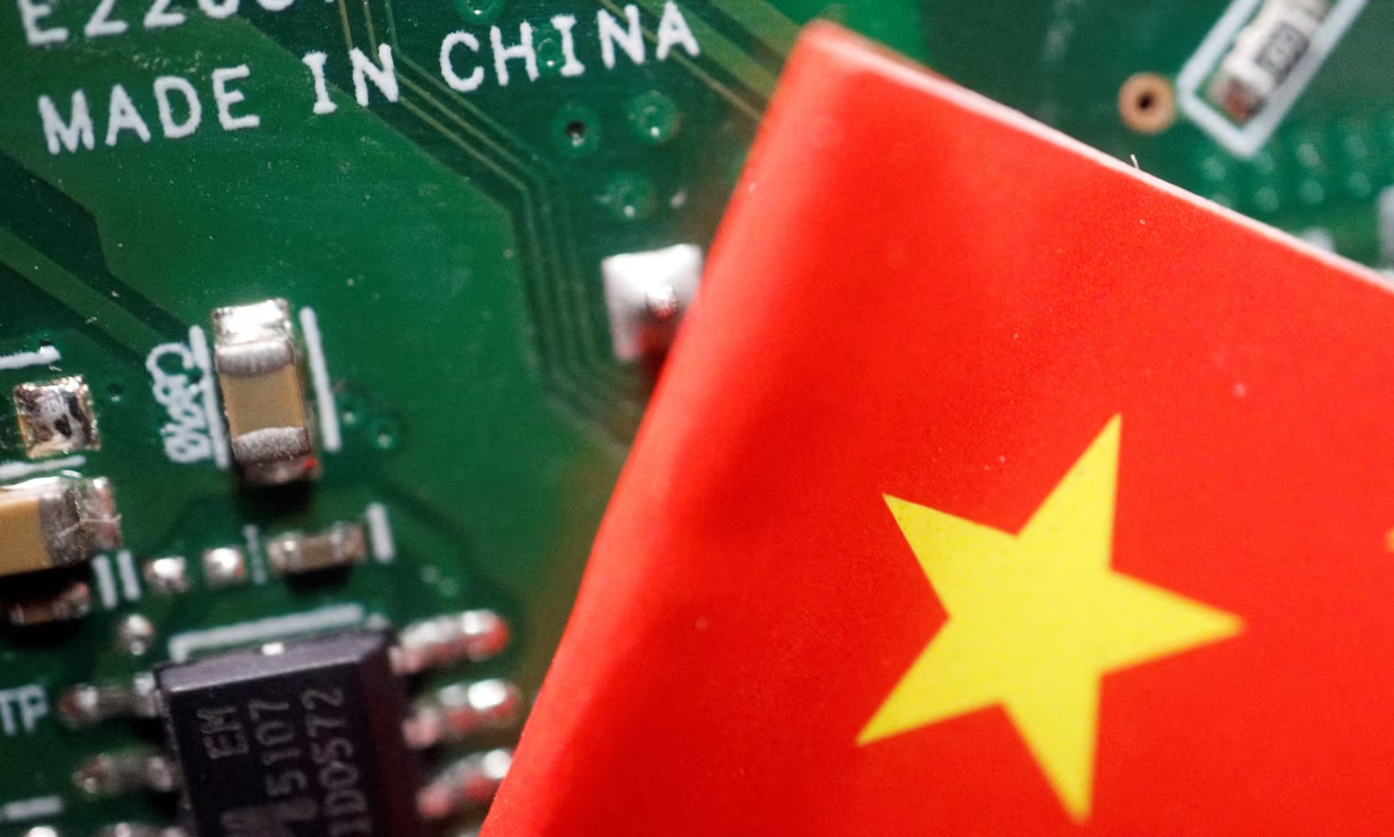
Prototipo EUV cinese arriva in anticipo
Con il progresso delle tecniche di calcolo sono stati inventati chip sempre più avanzati. I nodi di ultima generazione da 3 nm e 2 nm sono così piccoli che la normale lunghezza d’onda della luce è semplicemente troppo grande per imprimere in modo affidabile strutture di queste dimensioni.
Questo non è nuovo, poiché l’industria ha a lungo utilizzato la luce DUV (Deep UltraViolet) per eseguire la litografia sui wafer di silicio. Ma per raggiungere la scala nanoscopica dei design di chip più avanzati, era necessaria una sorgente luminosa a lunghezza d’onda ancora più corta.
Questa sorgente luminosa e metodo di litografia si chiama EUV (Extreme UltraViolet).

Fonte: Zeiss
Fino a poco tempo fa, l’EUV era monopolio della società olandese ASML (ASML ), l’unico produttore al mondo di macchine per litografia EUV.
Nel 2019, i chip a nodo 7nm di TSMC sono stati realizzati con il primo processo EUV, fornendo al mercato prodotti ad alto volume per i clienti.
Il controllo sull’accesso alla tecnologia EUV è stato centrale nelle sanzioni statunitensi contro l’industria dei semiconduttori cinese. Già nel 2018, gli Stati Uniti hanno iniziato a fare pressione sui Paesi Bassi per bloccare ASML dalla vendita di macchine EUV, componenti correlati e servizi di manutenzione.
L’idea era che limitare l’accesso all’EUV avrebbe rallentato la capacità della Cina di produrre chip all’avanguardia e, insieme ai limiti sull’esportazione di acceleratori AI avanzati, aiutasse gli USA a mantenere un vantaggio nella corsa all’IA.
Ma ora sembra che la spinta della Cina per l’indipendenza dei semiconduttori si sia accelerata sotto pressione, e Reuters riferisce che la Cina ha completato un prototipo di macchina EUV. Se lo sviluppo rimane in linea, potrebbe iniziare a produrre chip già nel 2028, con una successiva crescita della produzione.
Non solo ciò potrebbe complicare gli sforzi occidentali per limitare l’accesso della Cina alla produzione di punta, ma potrebbe anche rappresentare una minaccia a lungo termine alla catena di approvvigionamento dei semiconduttori, tradizionalmente centrata sull’Occidente—arrivando anni prima di quanto molti analisti ottimisti sulla Cina avessero previsto.
La inaspettata svolta EUV della Cina sfida il monopolio di ASML, indebolisce la strategia delle sanzioni occidentali e segnala un cambiamento a lungo termine nel potere globale dei semiconduttori.
Come funziona realmente la litografia EUV
Ciò che rende l’EUV così particolare, e spiega perché per molti anni sia rimasta un monopolio di ASML, è che non si tratta di una singola tecnologia, bensì dell’integrazione di numerosi capolavori di ingegneria ultraprecisa in un unico sistema.

Il primo elemento è un laser a CO2 ultrap potente da circa 30 kW, uno dei laser industriali pulsati più potenti al mondo. Nelle macchine ASML è prodotto dalla società tedesca Trumpf.
Non è però questo laser a produrre la luce EUV: esso fornisce l’energia. Per generare l’EUV, il sistema surriscalda minuscole gocce di stagno fuso trasformandole in plasma; le macchine ASML sparano circa 50.000 gocce di stagno al secondo.
Il plasma deve raggiungere temperature estreme, spesso indicate attorno ai 220.000 °C (360.000 °F), creando condizioni molto più calde della superficie del Sole e spingendo l’ingegneria industriale ai suoi limiti.
L’intero processo deve inoltre avvenire in un vuoto quasi perfetto, perché l’aria, come la maggior parte dei materiali, assorbe la luce EUV.

Fonte: SemiEngineering
E non è ancora tutto. La luce EUV deve poi essere diretta, modellata e focalizzata con una precisione sorprendente per incidere i wafer di silicio più avanzati, nei quali si parla spesso di densità prossime a 100 milioni di transistor per millimetro quadrato.
Questi specchi curvi, sviluppati dal leader tedesco dell’ottica Zeiss, devono essere fabbricati e allineati con una precisione prossima alla scala atomica.
«Se si ingrandisse uno specchio EUV fino alle dimensioni della Germania, la maggiore irregolarità, per così dire lo Zugspitze, sarebbe alta appena 0,1 millimetri.»
La precisione è talmente estrema che l’accuratezza direzionale degli specchi viene spesso spiegata con paragoni molto vividi. Se uno specchio EUV fosse usato per dirigere un fascio verso la Luna, in teoria sarebbe abbastanza preciso da colpire sulla superficie lunare un oggetto piccolo come una pallina da ping-pong.
Questi elementi ottici sono inoltre rivestiti da una pila multistrato, spesso composta da materiali alternati come silicio e molibdeno, in cui ogni strato è spesso soltanto pochi atomi.
«Qui vengono sovrapposti fino a 100 strati. Un singolo strato rifletterebbe appena l’un per cento della luce: la perdita sarebbe eccessiva.
Il risultato è una riflettività che permette di utilizzare fino al 70% della luce.»
Infine, lo stesso wafer di silicio deve muoversi e allinearsi con una precisione straordinaria. I sensori misurano continuamente la posizione e il piano portawafer deve mantenerla resistendo alle deformazioni causate dalle variazioni termiche e dai movimenti ad alta velocità.
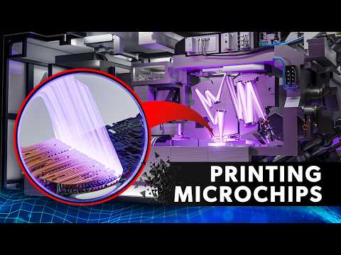
Considerando tutti questi passaggi, e tenendo presente che la spiegazione precedente resta una semplificazione, diventa chiaro perché replicare l’EUV sia così difficile: non basta riprodurre un progetto, ma occorre ricreare un vasto ecosistema di materiali, metrologia, controlli, ottica, sistemi a vuoto e produzione ultrapulita, integrato in un’unica macchina.
Perché è così difficile replicare l’EUV
Scorri per visualizzare →
| Sottosistema | Dominanza del fornitore | Perché è difficile |
|---|---|---|
| Sorgente di luce EUV (plasma di stagno) | ecosistema ASML + Trumpf | Laser ad alta potenza, sincronizzazione delle gocce, stabilità del plasma, mitigazione dei detriti |
| Ottica di proiezione | Quasi monopolio Zeiss | Perfezione della superficie a livello atomico, rivestimenti multistrato, resa su larga scala |
| Sistemi a vuoto | Molteplici fornitori specializzati | Integrità del vuoto ultra pulito con stadi in movimento e carichi termici elevati |
| Metrologia e sensori | Catena globale altamente specializzata | Circuiti di retroazione nanometrici in tempo reale; calibrazione, deriva, controllo della contaminazione |
| Software di controllo | Proprietario ASML | Integrazione stretta tra migliaia di sottosistemi; know-how di processo |
| Stadio e meccanica del wafer | Leader nella meccatronica di precisione | Accelerazione estrema senza vibrazioni; stabilità termica; ripetibilità su larga scala |
Il “Progetto Manhattan” EUV della Cina: Mobilitazione totale dei semiconduttori
Mobilitazione totale
Considerata l’importanza dei chip più avanzati nella competizione per l’IA, la robotica evoluta e le tecnologie militari, paragonare il programma EUV cinese a un Progetto Manhattan non è semplice retorica: ne riflette la portata e l’urgenza.
In primo luogo, sembra che nel più ampio programma per i semiconduttori siano confluite enormi quantità di capitale pubblico e privato: all’inizio del 2025 sarebbero stati mobilitati almeno 37 miliardi di euro, probabilmente affiancati da ulteriori fondi per ricerca universitaria, impianti industriali, sussidi ai fornitori critici, acquisti garantiti e domanda di futuri chip sostenuta dallo Stato.
Forse, inoltre, non avrebbe dovuto essere una sorpresa completa, dato che nel dicembre 2022 Huawei avrebbe depositato un brevetto relativo all’EUV.
Parallelamente, un’altra società cinese, SMIC, sarebbe riuscita a usare macchine DUV meno recenti per produrre chip della classe 5 nm senza EUV, mostrando quanto fosse forte l’incentivo ad arrangiarsi con strumenti limitati.
È stato esplorato anche un altro concetto: generare luce EUV mediante un acceleratore di particelle (sincrotrone), una direzione discussa già nel 2023 e collegata a una pubblicazione scientifica del 2022.
Tutti questi sforzi illustrano l’enorme importanza attribuita dalle istituzioni e dalle imprese cinesi sia alla padronanza dell’EUV sia alla creazione di alternative competitive che possano farne a meno.
Al centro di questi sforzi si trova Huawei, il colosso tecnologico cinese colpito da pesanti sanzioni.
Come l’acquisizione di talenti ha accelerato il programma EUV della Cina
Un altro tentativo di sbloccare la tecnologia EUV, più riservato, si sarebbe concentrato sull’acquisizione dell’esperienza e del capitale umano che ne hanno reso possibile lo sviluppo.
Gli ingegneri di punta, compresi alcuni ex dipendenti ASML ormai in pensione, sono stati obiettivi prioritari per il reclutamento. Secondo le indiscrezioni, fin dal 2020 sarebbero stati avvicinati anche altri dipendenti ancora in forza ad ASML.
Questi reclutamenti farebbero parte di una più ampia iniziativa per attirare in Cina i migliori talenti; già da anni agli esperti di semiconduttori attivi all’estero vengono offerti bonus d’ingresso e sussidi.
In alcuni casi isolati sembra che siano state adattate anche alcune norme nazionali per agevolare gli esperti assunti. Ad alcuni cittadini naturalizzati di altri Paesi, per esempio, sarebbero stati rilasciati passaporti cinesi consentendo loro di mantenere la doppia cittadinanza, benché la Cina la vieti ufficialmente.
Il fatto che molti di questi ingegneri siano di nazionalità o origine cinese potrebbe inoltre averne facilitato il reclutamento.
Nel complesso, l’affermazione secondo cui la Cina si limiterebbe a rubare tecnologie è spesso una semplificazione eccessiva di un ecosistema di ricerca e ingegneria in rapida crescita. In questo caso specifico, tuttavia, l’intersezione con i segreti industriali di ASML potrebbe essere rilevante.
All’interno del primo prototipo di litografia EUV della Cina
L’assunzione di ex dipendenti ASML, la reingegnerizzazione di componenti EUV e lo sviluppo indipendente di alternative nazionali sembrano aver prodotto un prototipo molto più grande dei tipici sistemi EUV ASML da 180 tonnellate, grandi quanto uno scuolabus: secondo le notizie occuperebbe un intero piano di fabbrica.
Ciò potrebbe indicare che il prototipo consuma più energia, è meno compatto o efficiente, oppure si trova semplicemente in una fase di ottimizzazione precedente rispetto ai progetti produttivi di ASML.
Componenti recuperati da vecchie macchine ASML, insieme ai mercati dell’usato per i ricambi dei suoi fornitori, potrebbero aver contribuito ad assemblare un prototipo funzionante mentre la produzione nazionale aumenta o migliora in qualità.
Un componente fondamentale che potrebbe ancora mancare, ed è eccezionalmente difficile da replicare con prestazioni analoghe, è l’ottica Zeiss. Sarebbe questa una delle ragioni per cui la macchina non può ancora produrre chip al livello desiderato.
High-NA EUV: la prossima frontiera nella corsa ai chip
Se ASML ha impiegato decenni a sviluppare l’EUV, la comparsa di un prototipo cinese suggerisce che il recupero del divario, almeno nella dimostrazione di un sistema di base, potrebbe avvenire molto più rapidamente di quanto molti ritenessero.
Ciò mette sotto pressione i leader occidentali dei semiconduttori, spingendoli ad accelerare verso la generazione successiva: l’EUV High-NA, cioè ad alta apertura numerica.
L’EUV High-NA è già in fase di prova presso aziende come Intel (INTC ) ed è stata valutata da Samsung e TSMC. Intel ha indicato pubblicamente il 2028 circa come obiettivo per i volumi produttivi, mentre TSMC e Samsung appaiono più caute e riservano l’EUV High-NA ai futuri nodi inferiori a 2 nm, senza affrettarne l’introduzione nella produzione di massa.
«Quanto più ampi sono gli angoli dai quali il sistema ottico raccoglie la luce, tanto più fini sono i dettagli visualizzati. Ciò significa che i sistemi ottici EUV diventano sempre più grandi.»
I sistemi High-NA impiegano elementi ottici ancora più grandi, che potrebbero offrire ad ASML un vantaggio durevole grazie al partner Zeiss.

Fonte: Zeiss
Uno specchio per la litografia EUV High-NA è circa due volte più grande e dieci volte più pesante degli attuali specchi EUV, rendendo l’intero sistema ancora più grande, pesante e complesso.
«Gli oltre 40.000 componenti dell’ottica di proiezione per la litografia EUV High-NA pesano circa dodici tonnellate per garantire una messa a fuoco ad alta precisione: sette volte il volume e il peso dell’ottica EUV consolidata.»
Cosa significa per gli investitori?
Nel breve termine, probabilmente cambia poco. La macchina EUV cinese sarebbe ancora soltanto un prototipo e non è chiaro quanto dipenda da componenti ASML riutilizzati o recuperati e quanto invece da parti interamente prodotte in Cina.
Tuttavia, è difficile presumere che la Cina fallirà per sempre. Con un numero sufficiente di specialisti, finanziamenti e tempo, non vi è una ragione evidente per ritenere che le istituzioni cinesi non possano infine replicare gran parte delle capacità EUV, soprattutto mentre matura il più ampio ecosistema di componenti, materiali e metrologia.
Anche lo scetticismo sulla capacità cinese di sostituire uno specifico componente, come gli specchi Zeiss, va trattato con cautela. Analisi analoghe sostenevano in precedenza che la Cina fosse indietro di oltre 15 anni, eppure ora è stato segnalato un prototipo.
Nel lungo periodo, da cinque a dieci anni, la Cina potrebbe costruire una catena di fornitura dei semiconduttori parallela e indipendente non soltanto a livello di fonderie, ma anche nella produzione delle apparecchiature.
Inizialmente, la produzione nazionale avanzata darebbe probabilmente priorità alla domanda interna, riducendo le vendite alla Cina di chip avanzati, strumenti produttivi e componenti di supporto.
Con il tempo, ciò potrebbe comprimere il fatturato e i margini dei produttori e fornitori occidentali di apparecchiature per semiconduttori, limitandone la capacità di reinvestire in ricerca e sviluppo ai livelli precedenti.
Ancora più preoccupante per aziende come ASML e altri produttori di apparecchiature, e persino per le fonderie, è che i chip avanzati prodotti in Cina potrebbero infine competere direttamente sui mercati esteri, soprattutto nelle reti commerciali in espansione dei BRICS e dell’Organizzazione per la cooperazione di Shanghai.
Mentre ASML e TSMC restano dominanti nel breve termine, i progressi cinesi nell’EUV introducono una pressione concorrenziale di lungo periodo che potrebbe rimodellare i mercati delle apparecchiature, delle fonderie e dei chip.
Conclusione
La comparsa di un prototipo EUV cinese con anni di anticipo rispetto alle aspettative di molti rappresenta un vero traguardo. Indica che i controlli alle esportazioni e le sanzioni difficilmente limiteranno in modo permanente le capacità tecnologiche in un settore nel quale l’Occidente gode da tempo di un vantaggio strutturale.
Nella migliore delle ipotesi, le restrizioni possono rallentare i progressi; nella peggiore, possono accelerarli creando un mercato interno protetto di circa 1,5 miliardi di persone, sostenuto dallo Stato e da una grande capacità industriale.
Ciò non significa che la Cina inizierà immediatamente a produrre chip all’avanguardia con strumenti EUV nazionali. Significa però che il percorso verso tale obiettivo è ora più chiaro, e probabilmente più rapido, di quanto molti ritenessero.
Nel complesso, ciò rafforza l’idea che la Cina si stia trasformando in una grande potenza tecnologica e non sia più soltanto la maggiore base manifatturiera mondiale.
Secondo alcune analisi, la Cina è ormai leader in un’ampia quota dei settori scientifici avanzati, mettendo in discussione la narrativa semplicistica secondo cui i suoi progressi deriverebbero soltanto dall’imitazione, anche se le controversie sui segreti industriali e i conflitti sulla proprietà intellettuale restano elementi reali di questa competizione.
Sebbene la svolta cinese modifichi l’orizzonte di lungo periodo, gli investitori alla ricerca di una posizione dominante immediata nel settore dei semiconduttori devono ancora guardare all’attuale leader del mercato.
Azienda di semiconduttori – TSMC
TSM Grafico dei prezzi
L’ascesa della Cina come potenza tecnologica è strategicamente importante, ma per ora le sue apparecchiature per la produzione di semiconduttori sembrano ancora inferiori, o appena prossime, ai sistemi occidentali più avanzati.
Nel settore delle fonderie, quindi, la disciplina di processo, l’apprendimento volto a migliorare le rese e l’esperienza operativa resteranno probabilmente decisivi nel prossimo decennio.
In definitiva, la produzione di semiconduttori è dominata da competenze di nicchia e dalla capacità di produrre su larga scala per ridurre i costi. Nessuna azienda ha perfezionato questo modello meglio di TSMC, leader taiwanese nella fabbricazione di chip ultra-avanzati.
TSMC produce principalmente chip di silicio, compresi i più potenti nodi da 3 nm e i futuri nodi della classe 2 nm. Poiché fabbrica i chip più avanzati e costosi, conquista una quota dominante del fatturato mondiale delle fonderie.

Fonte: Eric Flaningam
TSMC sta inoltre ampliando la capacità produttiva negli Stati Uniti, in particolare attraverso importanti investimenti negli stabilimenti dell’Arizona.
Con lo sviluppo dell’EUV High-NA già in corso, TSMC potrebbe mantenere per anni un vantaggio sui concorrenti cinesi come SMIC, soprattutto per resa, affidabilità e maturità della produzione in grandi volumi.
E anche dopo una concorrenza serrata con Samsung, Intel e altre fonderie, TSMC resta ben posizionata per difendere la propria leadership dall’ascesa dei concorrenti con sede in Cina, almeno nel futuro prevedibile.
Ultime notizie e sviluppi sul titolo TSMC (TSM)