전자
방사선 내성 칩이 CERN 가속기를 구동합니다

고방사선 환경을 위한 전자 장치 구축
Electronics are at the core of almost any technology invented in the past decades. As the world digitalizes even more processes and data, this is becoming more true every day.
하지만 일부 환경에서는 표준 전자 장치가 따라가기 어렵습니다. 그 중 하나가 입자 가속기입니다.
한편, 입자 가속기는 초당 수 테라바이트에 달하는 데이터를 생성하므로 초고효율 전자 부품이 필요합니다. 반면, 이들이 발생시키는 방사선 양은 전자 시스템을 혼란스럽게 만들기 쉽습니다.
Scientists at the CERN in Switzerland were faced with this dilemma. At the LHC particle accelerator at CERN, the world’s largest, radiations were emitted, making measurement difficult.
“우리는 표준 상용 부품을 테스트했지만 바로 고장났습니다. 방사선이 너무 강했습니다. 우리가 작동하는 무언가를 원한다면 직접 설계해야 한다는 것을 깨달았습니다.”
Rui (Ray) Xu, a Columbia Engineering PhD student
The first chip of this kind was developed in 2017 and put to the test in 2022 for the ATLAS experiments. ATLAS is the largest particle detector ever built, at 46 meters (150 feet) long and 25 meters (82 feet) in diameter.
The detectors contain 100+ million sensitive electronic channels to record the particles produced by the collisions. It contains many sub-detectors, each playing a separate role, to detect at the same time photons, electrons, muons, pions, etc.

출처: ATLAS
A second chip, the data acquisition ADC, has recently passed its final tests and is now in full production. It is fully described in a recently published paper1 in the journal IEEE Explore, under the title “A Radiation-Hard 8-Channel 15-Bit 40-MSPS ADC for the ATLAS Liquid Argon Calorimeter Readout”.
방사선이 전자 장치에 미치는 영향
Since the dawn of electronics, it has been known that radiation tends to damage electronic components and/or make them give out the wrong data.
Among the many effects radiation can have, the most problematic ones can be quickly listed:
- 트랜지스터 전압 변동으로 인해 데이터 오류가 발생하거나 트랜지스터 자체가 파괴됩니다.
- 메모리 부품에서 개별 비트(0 및 1)가 뒤바뀝니다.
- 집적 회로의 전기적 또는 열적 소손.
- 광 검출기와 광원 손상은 즉시 파괴하거나 수명을 단축시킬 수 있습니다.
This is a serious problem in high-radiation environments, like space, medical accelerators (radiation therapy, radiography), or nuclear facilities.
One option to solve the issue is simply to use enough shielding, putting the electronics part behind a protective layer, usually water or a heavy element like lead, depending on the type of radiation.
Another option is redundancy and error correction. If a component is in multiple copies, or a program runs several times, an error in only one of them can be detected and subsequently ignored.
The last option is to build electronics systems that are naturally resistant to radiation, which is the only option for electronic systems that have to be directly exposed to radiation, like the detectors of a particle accelerator.
| 방사선 효과 | 설명 | 영향 |
|---|---|---|
| 전압 임계값 변동 | 방사선이 트랜지스터 동작을 변화시킵니다 | 논리 오류 또는 부품 고장을 일으킵니다 |
| 단일 이벤트 업셋(SEU) | 메모리 또는 논리 회로에서 비트가 뒤바뀝니다 | 데이터가 손상되거나 시스템이 충돌할 수 있습니다 |
| 래치업 | 전하 입자에 의해 유도된 단락 | 칩을 영구적으로 손상시킬 수 있습니다 |
| 총 이온화 선량(TID) | 방사선 노출에 따른 점진적 악화 | 장치 수명을 감소시킵니다 |
방사선 방지 전자 장치 구축
상업적 실현 가능성
The problem the CERN engineers and scientists faced is that off-the-shelf components simply can’t survive the harsh conditions inside the accelerator.
At the same time, the market for radiation-resistant circuits is too small to entice investment from commercial chip manufacturers.
“최첨단 계측 장비 개발은 우리의 성공에 필수적입니다. 산업계는 그 노력을 정당화할 수 없었기에 학계가 나서야 했습니다.”
John Parsons – Professor of physics and leader of the Columbia University team working on the ATLAS detector.
In this specific case, the researchers needed to develop analog-to-digital converters (ADCs). These devices’ task is capturing electrical signals produced by particle collisions inside CERN’s detectors and translating them into digital data that researchers can analyze.
This is done through a device called a liquid argon calorimeter, which converts particle collisions into an electronic signal.
Columbia’s ADC chips convert these delicate analog signals into precise digital measurements, capturing details that no existing component could reliably record.
요구되는 조건
The researchers carefully chose and sized components and arranged circuit architectures and layouts to minimize radiation damage, as radiation shielding is not realistic in the particle detector.
게다가 해당 전자 보드는 운영 중에 접근할 수 없으며, 유지보수는 연 1회 정도만 가능하다는 점을 고려해야 했습니다.
구성 요소가 12년 운영 수명 동안 경험하게 될 방사선 수준은 일반적으로 정지 궤도 위성에서 마주치는 수준과 유사합니다.
Temporary errors can be tolerated, but permanent damage cannot be accepted, as it would hinder the work of all the research projects requiring ATLAS.
검증된 반도체 제조 기술 재사용
Reinventing how to produce semiconductors was not going to be a viable path to create a useful device within a reasonable budget and time frame.
따라서 연구원들은 CERN이 방사선 저항성을 검증한 상용 반도체 공정을 사용하고 혁신적인 회로 수준 기술을 적용했습니다.
A key decision in that respect was to rely on older, tried and tested lithography methods, using a commercial, triple-well 65-nm CMOS process for production of the ASIC custom chip (Application-Specific Integrated Circuit).
This 65 nm process is known to be inherently radiation hardened.
Another design choice was to minimize the components not directly present on the chip, reducing the risk of errors by integrating the chip’s internal clocks, memories, etc.

출처: IEEE Explore
하지만 보정 계산은 칩 외부에서 수행되어 방사선으로 인한 계산 오류가 발생해 잘못된 데이터를 초래하는 것을 방지합니다.
그들은 또한 방사선의 이온화 효과로 과충전될 수 있는 커패시터를 검토했습니다.
금속-절연체-금속(MiM) 커패시터는 기존의 금속-산화물-금속(MoM)보다 자연스럽게 30배~80배 얇으며, 크기도 절반이어서 방사선 및 고에너지 입자에 노출될 수 있는 표면을 감소시킵니다.

출처: IEEE Explore
최종 칩 설계 및 테스트
The final chip is an electronic design specifically designed to be optimal against radiation, instead of high-speed, ease of manufacturing, or boosted performance like commercial products.
총 45,617개의 칩이 ATLAS 검출기에 사용될 예정입니다.

출처: IEEE Explore
18개의 장치를 아날로그 성능에 대해 특성화했으며, 장기 아날로그 정확도 검증 및 광범위한 방사선 테스트 캠페인을 수행했습니다.
모든 결과는 이 칩이 ATLAS 검출기 환경에서 잘 작동할 것임을 보여주었습니다.
그럼에도 불구하고, 아무리 내성을 강화해도 이러한 방사선 수준은 모든 전자 시스템에 일부 오류와 문제를 일으킵니다. 따라서 연구원들은 실시간으로 오류를 자동 감지하고 수정하는 디지털 시스템을 구축했습니다.
보다 문제적인 이중 및 삼중 비트 오류는 모든 메모리 레지스터를 주기적으로 읽어 초기 프로그램과 비교함으로써 감지됩니다. 이러한 이중·삼중 오류가 발생한 측정값은 모두 폐기됩니다.
결론
This research project will enable the advanced analysis of high-energy particles generated by the LHC.
또한 “High Luminosity LHC” (HL–LHC와 함께 가속기의 주요 업그레이드에 핵심적인 요소가 될 것이며, 이 업그레이드는 LHC의 광도를 10배 향상시키는 것을 목표로 합니다.
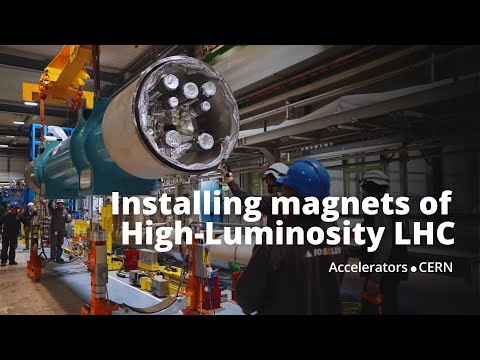
예를 들어, High-Luminosity LHC는 연간 최소 1,500만 개의 힉스 보존을 생산할 것이며, 이는 2017년 LHC가 생산한 약 300만 개와 비교됩니다.

출처: CERN
향후 CERN의 프로젝트, 예를 들어 Future Circular Collider (FFC)와 같이 2040년대 중반에 첫 실험이 시작될 경우에도 유사하거나 더욱 고도화된 방사선 방지 전자 장치가 필요할 가능성이 높습니다.
마지막으로, 기본 물리학을 위한 학술 예산으로 지원되는 이러한 프로젝트는 방사선 방지 전자 장치의 상업적 버전에 영감을 줄 수 있습니다.
인류가 영구적인 달·화성 기지 혹은 소행성 채굴과 같은 심우주 탐사를 모색함에 따라, 보다 내구성 있고 방사선 방지 전자 장치는 매우 유용할 것입니다.
첨단 센서에 투자하기
CEVA
(CEVA )
CEVA는 센서 기업으로 CERN과 파트너십을 맺어 기관의 알고리즘을 활용해 센서의 효율성과 전력 소비를 개선하고 있습니다. CEVA 솔루션과 IP(200개 특허)는 180억 대의 장치에 통합되어 있습니다.
이 회사의 솔루션은 전 세계 주요 전자 브랜드에서 널리 사용됩니다.

출처: CEVA
CEVA와 CERN 간 협력의 주요 적용 분야는 “Edge AI”이며, 이는 데이터 센터(클라우드)에서 멀리 떨어진 장치에 배치되어 소비자(에지) 가까이에서 동작하는 인공지능 애플리케이션을 의미합니다.
입자 물리학 알고리즘이 AI 애플리케이션에 재사용되는 것은 놀라운 일이 아닙니다. 예를 들어 신경망은 힉스 보존을 찾는 데 사용되었습니다. 입자 가속기 데이터 분석은 방대한 데이터가 빠르게 생성되기 때문에 클라우드가 아니라 현장에서 수행되어야 합니다.
CEVA는 CERN이 향후 실험에 사용할 수 있는 새로운 압축 알고리즘을 개발하도록 도왔으며, 이 새로운 기술을 자사 제품에 통합할 수 있게 되었습니다.
“CERN과의 협업 덕분에 우리는 네트워크가 16비트 기준 모델에 비해 최대 15배 빠르게 실행될 수 있는 혁신적인 접근 방식을 개발할 수 있었습니다.
이는 네트워크 속도를 향상시키고 에너지 소비를 최대 90% 절감하면서도 비슷한 정확도를 유지합니다.
This is but one of CEVA’s technological progresses, with the company active in wireless connectivity, sensors (vision, audio, motion), and neural network algorithms.

출처: CEVA
CEVA는 5G 연결(위성 5G 포함)과 사물인터넷(IoT) 및 임베디드 AI 솔루션이 결합된 추세로부터 큰 혜택을 얻으며, 산업 및 가정용 솔루션 모두에 적용됩니다. 또한 WiFi 6 솔루션의 선두주자이며 WiFi 7에서도 선도적인 위치를 차지하고 있습니다.

출처: Ruije
소프트웨어 및 IP 기업으로서 CEVA는 엔지니어들 사이에서 잘 알려져 있으며, IoT와 5G 분야에 관심 있는 투자자들에게 종종 간과됩니다.
CEVA는 데이터 처리와 Edge AI 분야에서 기술 진보의 최전선에 있는 흥미로운 기업이며, 이는 CERN이 인류가 수행한 가장 복잡한 데이터 분석 중 일부를 돕기 위해 CEVA를 선택한 사례에서 확인할 수 있습니다.
최신 CEVA(CEVA) 주식 뉴스 및 개발 현황
참조 연구:
1. Rui Xu; Jaroslav Bán; Sarthak Kalani; Chen-Kai Hsu; Subhajit Ray; Brian Kirby. A Radiation-Hard 8-Channel 15-Bit 40-MSPS ADC for the ATLAS Liquid Argon Calorimeter Readout. IEEE Explore. 28 May 2025. pp 180 – 199 DOI:10.1109/OJSSCS.2025.3573904
{
“@context”: “https://schema.org”,
“@type”: “FAQPage”,
“mainEntity”: [
{
“@type”: “Question”,
“name”: “왜 방사선 방지 전자 장치가 입자 가속기에 중요한가요?”,
“acceptedAnswer”: {
“@type”: “Answer”,
“text”: “방사선 방지 전자 장치는 CERN의 LHC와 같은 입자 가속기에서 필수적입니다. 높은 방사선 수준이 표준 칩을 손상시키고 데이터를 왜곡할 수 있기 때문입니다. 특수 칩은 이러한 극한 환경에서 신뢰할 수 있는 성능과 정확한 측정을 보장합니다.”
}
},
{
“@type”: “Question”,
“name”: “CERN에서 개발한 ADC 칩의 독특한 점은 무엇인가요?”,
“acceptedAnswer”: {
“@type”: “Answer”,
“text”: “CERN용으로 개발된 ADC 칩은 방사선 내성으로 알려진 65nm CMOS 공정을 사용해 제작되었습니다. 오류 정정, MiM 커패시터 및 맞춤형 아키텍처를 통합하여 10년 이상 고방사선 환경에서도 견딜 수 있습니다.”
}
},
{
“@type”: “Question”,
“name”: “CEVA는 CERN 실험에서 어떤 역할을 하나요?”,
“acceptedAnswer”: {
“@type”: “Answer”,
“text”: “CEVA는 CERN과 협력하여 입자 데이터 처리를 위한 Edge AI 및 압축 알고리즘을 최적화합니다. 이들의 기여는 실시간 데이터 분석에서 에너지 효율과 연산 속도를 향상시킵니다.”
}
}
]
}