
Computing
ASML (ASML): Hjørnestenen i moderne halvledere

 Føj Securities.io til dine foretrukne kilder på Google

Værktøjerne til chipfremstilling
Halvledere, og især computerchips, er hurtigt blevet en af verdens vigtigste teknologier og handelsvarer. Fra pc-æraens begyndelse over fremkomsten af smartphones og cloud computing til kunstig intelligens er chippenes betydning og efterspørgslen efter dem kun vokset.

Kilde: Applied Materials
Dette er en interessant industri, hvor ingen aktør er vertikalt integreret; i stedet er den sammensat af en konstellation af ultra-specialiserede virksomheder, som hver udfører et af de mange kritiske trin i at omdanne almindeligt sand (silicium) til tænkende maskiner.
De største virksomheder i sektoren er enten chipdesignere som Nvidia (NVDA ), eller “foundries”, der udfører den faktiske fremstilling af chips som TSMC (TSM ) (følg linket for dedikerede investeringsrapporter om disse virksomheder).
Disse virksomheder er stærkt afhængige af specialiserede leverandører til de maskiner, der kræves for at producere chipsene.

Kilde: ASML
Og ingen er vigtigere end virksomheden med et monopol på EUV (Extreme UltraViolet) litografi, den hollandske ASML.
ASML Prisdiagram
ASML’s rolle i fremstilling af halvledere
Hvordan litografi driver chipminiaturisering
ASML er specialist i litografimaskiner. Litografi betyder bogstaveligt »indgravering i sten« og er den proces, der indgraverer en processors node på en siliciumwafer og omdanner den til en computerchip.

Kilde: Nature
Jo mere avanceret chippen er, jo mindre er noden, og jo mere kompleks er litografiprocessen. Den kontinuerlige miniaturisering af noder og forbedring af litografi er det, der har gjort det muligt for computere at blive mere kraftfulde år efter år, i overensstemmelse med Moores lov.

Kilde: Steven Jurvetson
Litografi er ét trin i hele processen, der omdanner en silicium wafer til computerchips, med normalt 40-80x cyklusser for at fremstille en fuld chip.

Kilde: ASML
En vigtig fysisk grænse for litografi er, at den indgraverede node ikke kan være større end bølgelængden af det kraftige lys, der bruges til at gøre det.

Kilde: ASML
Så efterhånden som transistorerne blev mindre, kræves højere og højere frekvens af lys, i dag gående mere og mere ind i den øvre ende af ultravioletspektrummet.
Det første skridt ud af det synlige lysspektrum var med I-line, efterfulgt kort tid efter af DUV (Deep Ultraviolet) litografi.

Kilde: Icometrue
Disse metoder bar industrien gennem en periode med stadig mere avancerede smartphones og datacentre. Til de mest avancerede værktøjer var der dog brug for en ny teknologi: EUV-litografi (ekstrem ultraviolet).
Hvad er EUV-litografi, og hvordan fungerer den?
EUV muliggør ultrakompakte noder på 7 nm, 5 nm, 3 nm og endnu mindre. Disse avancerede noder anses ofte for nødvendige til anvendelser som AI, maskinlæring, 5G, AR/VR og avancerede cloudtjenester.
ASML er førende inden for DUV-teknologi, men EUV er endnu vigtigere, fordi virksomheden er den eneste producent af EUV-maskiner til chipfremstilling. Nogle kinesiske virksomheder forsøger dog at komme ind på markedet så hurtigt som muligt, som beskrevet nedenfor.
EUV-teknologi er ekstremt vanskelig at beherske på grund af en række tekniske begrænsninger:
- Processen foregår i et vakuummiljø, fordi næsten alt absorberer EUV-lys.
- Den kræver en meget stærk energikilde i form af en kraftfuld laser, med op til 40 kW laser i brug. Denne type laserforstærker kræver 7,3 kilometer kabel, vejer 17 ton og indeholder over 450 000 dele.
- Laseret exciterer små dråber af tin på 25 mikrometer i diameter, med 50 000 dråber, der falder per sekund.
- Tinnet fordampes derefter til en plasma af laserens kraft, hvilket udsender EUV-lys.

Kilde: Semi Engineering
Hvert af disse trin kræver ekstremt avanceret måling, værktøjer, kontrol og sensorer, alting med en præcisionskvalitet målt i mikrometer og nanosekunder.
Gennem dyb ekspertise opbygget i årtier med at bygge litografimaskiner, er ASML (så langt?) den ubestridte mester i EUV-teknologi. De har også opbygget et tæt netværk af nøgleleverandører, med f.eks. spejle på op til 1 meter i tværs, med overfladeslæthed ned til picometer (en billiontedel af en meter).
Udover de meget præcise maskiner kræver EUV også specialiseret og proprietær software til kalibrering, diagnostik, evaluering og automatisering.
Selvom EUV uden tvivl er fremtiden for virksomheden og en stor del af dens indtægter, udgør mindre avancerede DUV-fremstillede chips stadig størstedelen af verdens samlede halvlederproduktion.

Kilde: ASML
ASML
ASML virksomhedsoverblik & nøglemålinger
Virksomheden blev grundlagt i 1984 som et joint venture mellem de hollandske virksomheder ASM og Philips. I dag beskæftiger den mere end 44.000 personer fordelt på 60 lokationer. ASML har samarbejdet med TSMC fra begyndelsen og leverede allerede i 2004 litografiteknologi til 90 nm-noder.
I 2011 leverede ASML litografimaskiner til 32 nm-noder. På det tidspunkt kostede en litografimaskine i gennemsnit 27 mio. euro.
I 2022 havde virksomheden solgt 140 EUV-maskiner til en pris på over 200 mio. dollar stykket. Det krævede tre Boeing 747-fly at transportere én af de 180 ton tunge maskiner.
ASML-målinger
I 2024 omsatte ASML for 28,3 mia. euro ved at sælge 583 litografimaskiner. Virksomheden har en bemærkelsesværdig bruttomargin på 51,3 %, hvilket gør det muligt at geninvestere 4,3 mia. euro i forskning og udvikling, næsten dobbelt så meget som i 2020.

Kilde: ASML
Virksomheden forventer, at omsætningen vokser til 44-60 mia. euro i 2030, med en bruttomargin på 56-60 %.
ASMLs brancheførende resultater inden for litografi har givet aktionærerne store afkast. I 2024 blev 3 mia. euro sendt tilbage til aktionærerne, og udbyttet er tredoblet siden 2018.

Kilde: ASML
Virksomheden har klaret sig markant bedre end Nasdaq som helhed gennem de seneste 15 år, selv om perioden generelt var meget gunstig for teknologiaktier, og udviklingen har fulgt de overordnede halvlederindeks.

Kilde: ASML
ASML forventer, at den installerede base af litografimaskiner fortsætter med at vokse frem mod 2030, hvilket vil øge indtægterne fra vedligeholdelse, service og opgraderinger betydeligt.

Kilde: ASML
EUV-maskinerne sælges ikke i størst antal, men de tegner sig for halvdelen af virksomhedens omsætning på grund af den højere pris.
Det meste af salget i slutningen af 2024 og begyndelsen af 2025 gik til Taiwan, Sydkorea, USA og Kina. Salget i Taiwan kan generelt antages hovedsageligt at gå til TSMC, i Sydkorea til Samsung og i USA til TSMC, som åbner et nyt støberi i Nevada, samt til Intel (INTC ).

Kilde: ASML
Salget til Kina var tidligere langt større, men amerikanske sanktioner mod Kina og kinesiske chipproducenters forsøg på at skifte til lokale leverandører har reduceret ASMLs salg i landet til ældre litografiteknologier.
ASML’s risici på det kinesiske marked & sanktionseffekt
Sanktionkrige
Kina er sammen med Taiwan en af verdens største halvlederproducenter, og ASML havde derfor tidligere et betydeligt salg på dette marked.
Flere års tiltagende spændinger og stadig hårdere sanktioner mod den kinesiske halvlederindustri fra skiftende amerikanske regeringer har imidlertid ændret markedet drastisk for ASML.
I sommeren 2022 forbød USA eksport af EUV-maskiner til Kina. Det var muligt, fordi ASML trods sin hollandske oprindelse er afhængig af central amerikansk immateriel ejendom i produktionen af litografimaskinerne.
Senere blev selv eksporten af DUV-maskiner som ASMLs TWINSCAN NXT:1980Di begrænset, så Kina kun fik adgang til mindre avanceret DUV-teknologi. Denne sanktionsrunde skyldtes blandt andet Huaweis nylige succes med at producere avancerede chips uden EUV-maskiner i september 2023.
Kinesiske løsninger
Huawei arbejder på egne EUV-løsninger og indsendte allerede et patent i december 2022.
En anden kinesisk virksomhed, SMIC, har formået at bruge ældre DUV-maskiner til at fremstille 5 nm-chips uden EUV.
»Det krævede flere på hinanden følgende trin med litografi og ætsning, især SAQP, for at efterligne EUV-teknologiens præcision. Metoden er langsommere, mere fejlbehæftet og dyrere, men den virker.«
Både SMIC og Huawei arbejder også på at fremstille 3 nm-chips ved hjælp af selvjusterende firedobbelt mønsterdannelse (SAQP). Huawei udvikler desuden et 3 nm-chipdesign, hvor silicium erstattes af kulstofnanorør.
Endelig kan kinesisk fremstillede EUV-maskiner snart komme på markedet, i første omgang til indenlandsk brug. Et andet alternativ kan være at skabe EUV-lys med en partikelaccelerator i stedet for tinplasma, en idé der allerede blev diskuteret i 2023 på baggrund af en videnskabelig artikel fra 2022.
En risiko for ASML?
På længere sigt er det sandsynligt, at ASML mister det kinesiske marked, fordi landet ikke kan være afhængigt af vestlig teknologi og derfor må genopbygge en hel parallel forsyningskæde for halvledere fra bunden.
Indtil videre handler dette mere om strategisk rivalisering mellem USA og Kina end om en forretningsmæssig trussel mod ASML.
Det skyldes flere forhold:
- Salget af DUV-maskiner til Kina udgør kun en mindre del af ASMLs samlede omsætning.
- Metoder, der omgår EUV ved hjælp af den ældre DUV-teknologi, kan teknisk set lade sig gøre. De er dog mindre pålidelige og giver derfor dyrere chips.
- Det kan være en brugbar løsning for Huawei og andre kinesiske elektronikvirksomheder uden adgang til avancerede chips, men metoderne er ikke økonomisk konkurrencedygtige på internationale markeder.
- EUV-maskiner fremstillet af Huawei vil kræve omfattende forbedringer og finjustering. De vil desuden kun blive produceret i et begrænset antal, som i mange år højst vil kunne dække den indenlandske kinesiske efterspørgsel.
- EUV-generering med en cyklotron er stadig i høj grad teoretisk. Det vil tage år eller måske årtier, før den kan blive et brugbart alternativ til den EUV-teknologi, der anvendes i dag.
Non-EUV-salg
Uafhængigt af Kinas forsøg på at udvikle EUV-maskiner vil salget af DUV sandsynligvis forblive stabilt. EUV er blevet standarden for de mest kritiske lag i LOGIC- og DRAM-chips, men alle øvrige lag fremstilles fortsat med DUV-teknologi.
ASMLs stærke position inden for DUV sikrer derfor stabile indtægter, herunder fra service og vedligeholdelse af den eksisterende maskinpark, hvor hver maskine kan være i drift i mere end 20 år.
Udviklingen og udbredelsen af EUV er dermed vigtig, men ikke afgørende for virksomhedens udsigter på kort sigt.
Det samme gælder tilknyttede systemer til litografimaskiner, såsom sensorer og metrologi til måling og kvalitetskontrol af det færdige produkt.

Kilde: ASML
| Teknologi | Node-størrelse | Typisk brug | Vigtigste begrænsning |
|---|---|---|---|
| DUV | 14nm–90nm+ | Ældre chips, ikke-kritiske lag | Ikke egnet til de mindste noder |
| EUV | 7nm–3nm | Avanceret logik, DRAM | Kompleks, dyr, høj energi |
| High-NA EUV | 2nm og mindre | Næste generations højtydende chips | Højere omkostninger, begrænset udrulning |
Fremtiden for litografi
ASML fortsætter med at innovere og opkøber aktivt nye nøgleteknologier. Et eksempel er købet af producenten af optisk glas Berliner Glas Group i 2020, som hjælper virksomheden med at udvikle næste generation af maskiner til chipfremstilling.

Kilde: ASML
Kinesiske konkurrenter kan komme med EUV-løsninger i kommerciel skala i de kommende år. ASML arbejder dog allerede på næste trin, kaldet High-NA-litografi. »NA« står for numerisk apertur, et mål for hvor meget lys et optisk system kan indsamle og fokusere.
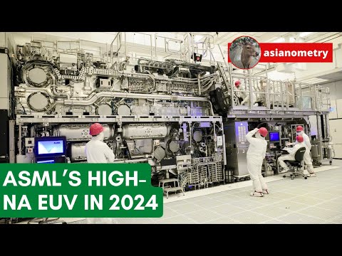
ASML gør hurtige fremskridt med teknologien. Den seneste optiske innovation danner grundlag for virksomhedens EUV-køreplan mod stabilitet på pikometerniveau, svarende til 1/200 af et siliciumatom, på asfæriske spejle.
High-NA EUV-optik skal bidrage til en EUV-platform med højere produktivitet og kan dermed løfte EUV-teknologiens ydeevne og produktivitet langt ind i det næste årti, efter 2030.

Kilde: ASML
High-NA-teknologien skal ikke kun være mere præcis og hurtig, men også mere energieffektiv. Det bliver stadig vigtigere, efterhånden som kraftigere litografimaskiner medfører store energiudgifter.
High-NA EUV bliver sandsynligvis metoden til masseproduktion af chips med 2 nm-noder og mindre.

Kilde: ASML
Intel var tidligt ude med at tage High-NA EUV i brug på sit støberi i Oregon. Teknologien er stadig ved at blive indført i støberierne, og andre teknologier som ætsning kan også få betydning for fremtidige forbedringer af ydeevnen.
»Med tilføjelsen af High-NA EUV får Intel branchens mest komplette værktøjskasse til litografi. Det gør virksomheden i stand til at udvikle fremtidige procesteknologier videre fra Intel 18A og ind i anden halvdel af dette årti.«
»Prisen på 400 mio. dollar pr. maskine« får også nogle støberier til at udskyde indførelsen med mindst én chipgeneration.
High-NA EUV bør dog være et forholdsvis enkelt næste skridt for ASML, fordi teknologien genbruger en stor del af den viden og erfaring, der gennem de seneste 20 år gjorde den »almindelige« EUV-teknologi mulig.
Hvorfor prioriterede vi fælles komponenter og modulopbygning i alle vores EUV-litografisystemer? Fordi alle systemerne dermed får gavn af erfaringerne fra 20 års udvikling af EUV.
Gennemprøvet teknologi mindsker risikoen for fejl, og modulerne gør det lettere at installere og integrere systemet i kundens chipfabrik.
Konklusion
Gennem en kompromisløs indsats for størst mulig præcision og teknisk ekspertise er ASML blevet selve litografivirksomheden og dominerer sit nichemarked.
Virksomheden har i praksis monopol på EUV, den vigtigste teknologi til fremstilling af alle de mest avancerede chips, der kræves til udviklingen af AI-teknologier, førende datacentre og de nyeste generationer af smartphones.
Hvis USA ikke havde forbudt eksport af EUV til Kina, ville ASML sandsynligvis uden større problemer være forblevet den eneste centrale leverandør af teknologien i et eller to årtier.
Sanktionerne og investeringer på titals milliarder i det, der er blevet en strategisk sårbarhed, kan en dag gøre kinesiske producenter til alvorlige konkurrenter til ASML. De halter dog stadig bagefter og må nøjes med DUV-maskiner, lavere udbytte og højere omkostninger.
De håber samtidig, at en kinesisk fremstillet EUV-maskine snart kan blive et bedre alternativ. Når Huawei og SMIC når op på niveauet for EUV-teknologi fra 2025, vil ASML sandsynligvis allerede være i gang med at udrulle High-NA EUV.
Man bør ikke undervurdere Kinas evne til at indhente forspringet og opbygge en indenlandsk forsyningskæde, men den bør heller ikke overvurderes. Som situationen er nu, står ASML til at forblive førende inden for litografi til avanceret chipfremstilling i mindst de næste ti år og konkurrencedygtig langt længere.
ASML har også en meget stærk position inden for DUV og metrologi, som giver ekstra indtægter til finansiering af virksomhedens forsknings- og udviklingsbudget.
Ud over virksomhedens kvalitet er værdiansættelsen det sidste spørgsmål, investorerne må tage stilling til. På grund af monopolstillingen og sektorens generelle vækst indregner ASML-aktien allerede en stor del af den fremtidige vækst.
Det virker rimeligt, men betyder også, at værdiansættelsen langt fra er billig: ASMLs kurs/indtjeningsforhold har ligget mellem et »lavt« niveau på 20 og helt op til 54.
Seneste ASML (ASML) aktienyheder og udviklinger



