Computing
Lithography na Walang Maskara: Isang Game Changer para sa mga Tagagawa ng Chip

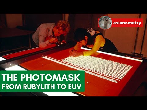
Lithography, Ang Puso ng Paggawa ng Semiconductor
Producing semiconductors has become one of the most profitable and strategic industrial activities in the 21st century, with companies like Nvidia (NVDA ), Intel (INTC ), or TSMC (TSM ) (follow the links for a dedicated report on each of these companies) reaching market capitalization in billions if not several trillions of dollars.
Karamihan sa kanila ay gumagamit ng prosesong tinatawag na photolithography. Tulad ng pangalan, gumagamit ito ng napakalakas na sinag ng ilaw upang iukit ang mga silicon wafer at gawing mga computer chip at iba pang semiconductor component.
Kinakailangan nito ang napaka-espesyal na mga makina na may maraming ultra-precise na lente, motor, at isang sistema na tinatawag na “photomask”.

Pinagmulan: CopperPod IP
Ang mga photomask ay gawa sa quartz o glass substrate na may balot na opaque film kung saan inukit ang pattern ng device na ginagawa. Ang film na ito ay essentially ang template para sa mga chip na iukit sa silicon wafer, bagaman ito ay miniaturized sa mas maliit na sukat sa proseso ng pag-ukit.
Karamihan ng mga chip ay ginagawa gamit ang DUV (Deep Ultra-Violet) lithography machines, na gumagamit ng malalakas na UV beam upang i-etch ang silicon. Ang mas advanced na mga chip ay gumagamit ng EUV (Extreme Ultra-Violet), na gumagamit ng mas masidhing UV light. Sa kasalukuyan, ang semiconductor manufacturer na ASML (ASML ) ay may monopolyo sa EUV.
Ang parehong DUV at EUV machines ay malaki, mahal, at kumakain ng maraming enerhiya.
Isang alternatibo ang umuusbong sa maskless lithography. Maaaring nakagawa ang teknolohiyang ito ng malaking pagtalon pasulong dahil sa unang deep-UV microLED display chips sa mundo na inimbento ng mga Chinese researcher.
Working at the Hong Kong University of Science and Technology and the Southern University of Science and Technology at Shenzhen, they published their results in Nature Photonics under the title “High-power AlGaN deep-ultraviolet micro-light-emitting diode displays for maskless photolithography1”.
Lithography na Walang Maskara
Ang pangunahing punto ng paggamit ng photomasks para sa lithography ay nagbibigay-daan ito sa DUV machine na gumamit ng maraming ilaw, at pagkatapos ay i-focus ang bahagi nito sa proseso ng pag-ukit. Gayunpaman, nagdudulot ito ng mababang light efficiency, hindi sapat na optical power density, at sa huli ay mababang kahusayan at mataas na konsumo ng enerhiya.
Isang alternatibo ay ang paggamit ng mas tumpak na UV light source, tulad ng aluminum gallium nitride deep-ultraviolet (UVC) micro-light-emitting diodes (micro-LEDs). Subalit, ang pag-develop ng UVC LEDs na may sapat na power output ay naging isyu hanggang ngayon.
Ibig sabihin, ang maskless lithography ay nagamit lamang para sa mga substrate na may mababang resolusyon, tulad ng printed circuit boards, sa halip na chip-grade silicon wafers.
Ang maskless photolithography ay magbabawas nang malaki sa gastos ng paggawa ng semiconductor at mag-aalok ng mas maraming opsyon sa customization. Sa pangkalahatan, gagawing mas mura at mas madaling gawin ang anumang elektronikong produkto ang teknolohiyang ito.
Mas Magandang UVC LEDs
Isang pangunahing salik sa underperformance ng UVC micro-LEDs ay ang malalaking alignment gaps sa panahon ng fabrication processes ng LED sub-units na nagdudulot ng problema kapag sinusubukang buuin ang malalaking UVC micro-LED display. Hindi lamang maaaring hindi uniform ang ilaw ng isang partikular na LED internally, kundi iba-iba rin ang katangian ng mga LED na ginawa nang sabay-sabay.

Pinagmulan: Nature Photonics
Pinabuti ng mga mananaliksik ang fabrication method upang matagumpay na makabuo ng uniform na 160 × 90 UVC micro-LED array. Ang array na ito ay may pixel size na 6 μm at pitch na 10 μm.

Pinagmulan: Nature Photonics
Pagpapakinabangan ng UVC LEDs
Ang mga pinabuting LED ay pagkatapos na-integrate sa mga circuit board upang lumikha at mag-project ng digital UV patterns.
Ang mga resultang sistema ay maaaring magpakita ng anumang komplikadong pattern at drawing sa matinding UVC light.

Pinagmulan: Nature Photonics
Dahil sa maliit na sukat ng mga LED, hindi na kailangan ang komplikadong demagnification lenses na ginagamit sa photolithography gamit ang photomasks.
Pagkatapos ng 5-segundong exposure, isang mirror-written na istruktura ang nabubuo sa ibabaw ng wafer. Maaari nitong iukit ang mga pattern na may sukat mula 3 μm hanggang 100 μm (micrometers).

Pinagmulan: Nature Photonics
Ang deep-UV microLED display chip na ito ay nag-iintegrate ng ultraviolet light source sa pattern sa mask. Nagbibigay ito ng sapat na irradiation dose para sa photoresist exposure sa maikling panahon, na lumilikha ng bagong landas para sa paggawa ng semiconductor.”
Pr. KWOK Hoi-Sing – Founding Director of the State Key Laboratory of Advanced Displays and Optoelectronics Technologies at HKUST
Karagdagang Pag-unlad
Mas Mahusay na UVC LEDs
Ang research team na responsable sa tagumpay na ito ay naniniwala na maaari nilang itulak pa ang performance ng kanilang micro-LEDs mula sa 320 × 140 prototype.
Nakikita nila ang landas upang makabuo ng 1k, 2k, o kahit 8k high-resolution deep ultraviolet microLED display screens, na mag-uukit ng mga pattern sa silicon nang mas eksaktong paraan.
“Kung ihahambing sa iba pang representatibong gawain, ang aming inobasyon ay may mas maliit na device size, mas mababang driving voltage, mas mataas na external quantum efficiency, mas mataas na optical power density, mas malaking array size, at mas mataas na display resolution.
Dr. FENG Feng – Postdoctoral research fellow at HKUST
Karagdagang Suporta na Sistema
Bagaman ang UVC-microLEDs ay hindi nangangailangan ng parehong hanay ng mga lente tulad ng klasikong lithography gamit ang photomasks, ang resolusyon ng mga mananaliksik ay hindi pa sapat.
Kaya, ang mga kaugnay na lens at focusing system, na lampas sa saklaw ng expertise ng mga mananaliksik sa LED manufacturing, ay maaaring makabuluhang magpabuti sa maskless photolithography. Gayunpaman, hindi ito dapat maging malaking teknikal na kahirapan para sa industriya ng semiconductor, dahil kilala at karaniwang ginagamit na teknolohiya ito.
Kaya, ang mga kumpanya na kasalukuyang gumagawa ng DUV machines ay madaling makakalikha ng bagong disenyo gamit ang maskless UVC microLEDs at focusing lenses sa halip na tradisyonal na disenyo na nangangailangan ng mamahaling photomasks.
Pamumuhunan sa Semiconductor Lithography
Habang nagiging mas karaniwan ang maskless lithography sa industriya ng semiconductor, ang teknolohikal na pag-shift na ito ay malamang magdulot ng ilang winners at losers.
Ang mga kumpanyang espesyalista sa paggawa ng photomask tulad ng Photronics, Inc. (PLAB ) ay malamang na masaktan.
Sa kabilang banda, ang mga kumpanyang gumagawa ng DUV lithography machines ay makikinabang mula sa bagong maskless na disenyo. Sa pag-alis ng mamahaling consumable, magiging mas mura ang buong operasyon ng lithography. Ang mas murang semiconductor ay magpapataas ng volume ng benta, na magpapalaki ng demand para sa DUV machines.
Maaari kang mag-invest sa mga kumpanyang may kaugnayan sa semiconductor sa pamamagitan ng maraming broker, at dito, sa securities.io, matatagpuan mo ang aming mga rekomendasyon para sa pinakamahusay na broker sa USA, Canada, Australia, UK, at marami pang ibang bansa.
O, kung mas gusto mo ang mas diversified na approach, maaari kang mag-invest sa mga semiconductor-related ETFs tulad ng iShares Semiconductor ETF (SOXX), ang VanEck Semiconductor ETF (SMH), o ang Global X Semiconductor ETF (SEMI).
Maaari mo ring alamin pa ang tungkol sa semiconductor manufacturing equipment supply chain at mga pangunahing kumpanya sa “Top 10 Semiconductor Equipment Stocks for Manufacturing Support”.
Kumpanya ng Semiconductor Lithography
ASML Holding N.V.
(ASML )
Pangkalahatang-ideya ng ASML
The world’s largest semiconductor equipment supplier by market cap, Dutch ASML is also the leader in the field, with a quasi-monopoly on a key technology called EUV lithography (Extreme UltraViolet).
EUV allows for ultra-small nodes, up to 7nm, or even 5nm and 3nm. These advanced node levels are often considered necessary for applications like AI, machine learning, 5G, AR/VR, and advanced cloud services.
EUV is currently at the center of the China-USA tensions and trade wars. In the summer of 2022, the USA banned the export of EUV machines to China. This was followed by efforts from Huawei to develop its own EUV solutions, with a patent deposited in Disyembre 2022.
By having a de facto monopoly on EUV out of China, ASML is a very prominent chip equipment manufacturer, a status heightened by the US pressure to restrict the export of the technology to its main rival. As a result, ASML is a crucial supplier to all chip manufacturers looking to build the most advanced chips.
EUV is the successor to previous technology, also sold by ASML, the DUV lithography (Deep UltraViolet).

Pinagmulan: ASML
EUV systems make up only a fraction of the machines sold, but at a much higher price, so a large part of revenues and profits. Still, DUV systems (ArFi, ArF, & KrF) represent the majority of the company sales (61%).

Pinagmulan: ASML
ASML is not the only DUV machine manufacturer, with competitors like Canon or Nikon active as well, but it is by far the most “focused” company, while its Japanese competitors are conglomerates with multiple other activities.
Mga DUV Machine at Tsina
Chinese competition is growing in DUV, due to the Chinese government’s push for domestic suppliers of semiconductor equipment.
Considering that improved UVC-microLEDs, the latest innovation in making maskless DUV more realistic, came from Hong Kong and Shenzhen researchers, this is something investors should take into account especially as China represents 47% of ASML’s revenues.
Exports of DUV machines to China have also been subjected to US sanctions, but these met significant pushback from the Dutch, Korean, and even Taiwanese governments.
Amsterdam has ruled that from now on ASML will be procuring the necessary license to export their DUV machines to members under the U.S. Bureau of Industry Standards’ Entity List from the Dutch government instead of the U.S. government.
This essentially means that the U.S.-mandated export controls will be under the licensing purview of administrators in the Netherlands instead of the United States.
Konklusyon Tungkol sa ASML
Still, despite potential China-related risks, ASML is the (almost) uncontested leader of the lithography industry and is already moving on to the next level of EUV technology: high-NA EUV systems (High Numerical Aperture).
High-NA EUV machines are now being deployed: to Intel in Disyembre 2023, to TSMC a year later, and to Samsung by 2025.
ASML also unveiled in the summer of 2024 its plans for what comes next: “Hyper-NA” EUV technology”. This concept, still in early research stages, would not be deployed until after 2030.

Pinagmulan: Tech PowerUp
Overall, ASML advances in EUV and expertise in DUV make it a likely winner in any tech war in fields afferent to its expertise, such as maskless DUV.
It might, however, see a period of instability and renewed competition with Chinese manufacturers likely to take market shares of the country’s semiconductor production, especially if helped by the Chinese government or because of US-ordered sanctions regarding ASML’s sales to China.
Sanggunian ng Pag-aaral:
1. Zhang, H., Li, D., Wang, Y., et al. (2024). High-power AlGaN deep-ultraviolet micro-light-emitting diode displays. Nature Photonics. https://doi.org/10.1038/s41566-024-01551-7


