
Υπολογιστική
ASML (ASML): Το Θεμέλιο των Σύγχρονων Ημιαγωγών

 Προσθέστε το Securities.io στις προτιμώμενες πηγές σας στο Google

Τα Εργαλεία της Κατασκευής Ενσωμάτων
Οι ημιαγωγοί, και ιδιαίτερα τα ολοκληρωμένα κυκλώματα, αποτελούν βασική τεχνολογία της σύγχρονης οικονομίας. Η ζήτηση αυξήθηκε στις εποχές των υπολογιστών, των έξυπνων τηλεφώνων, του υπολογιστικού νέφους και της τεχνητής νοημοσύνης, αλλά ο κλάδος παραμένει κυκλικός και η ανάπτυξη διαφέρει ανά τελική αγορά.

Πηγή: Applied Materials
Αυτή είναι μια ενδιαφέρουσα βιομηχανία, όπου κανένας παίκτης δεν είναι κάθετα ενσωματωμένος· αντίθετα, αποτελείται από έναν αστερισμό υπερ-ειδικευμένων εταιρειών, καθεμία από τις οποίες εκτελεί ένα από τα πολλά κρίσιμα βήματα στη μετατροπή του συνηθισμένου άμμου (πυριτίου) σε μηχανές που σκέφτονται.
Οι μεγαλύτερες εταιρείες του κλάδου είναι είτε σχεδιαστές τσιπ όπως Nvidia (NVDA ), ή «foundries» που κάνουν την πραγματική κατασκευή τσιπ όπως TSMC (TSM ) (ακολουθήστε τον σύνδεσμο για αφιερωμένες επενδυτικές αναφορές σε αυτές τις εταιρείες).
Αυτές οι εταιρείες εξαρτώνται σε μεγάλο βαθμό από εξειδικευμένους προμηθευτές για τις μηχανές που απαιτούνται για την παραγωγή των τσιπ.

Πηγή: ASML
Η ASML είναι ο μόνος προμηθευτής που έχει διαθέσει συστήματα λιθογραφίας EUV για εμπορική παραγωγή μεγάλου όγκου. Η θέση αυτή βασίζεται τόσο στη δική της τεχνολογία όσο και σε ένα εκτεταμένο δίκτυο εξειδικευμένων προμηθευτών.
ASML Διάγραμμα τιμής
Ο Ρόλος της ASML στην Κατασκευή Ημιαγωγών
Πώς η Λιθογραφία Τροφοδοτεί τη Μικροποίηση των Ενσωμάτων
Η ASML ειδικεύεται στα συστήματα λιθογραφίας. Η λιθογραφία μεταφέρει σχέδια κυκλωμάτων σε φωτοευαίσθητο υλικό πάνω σε δίσκο πυριτίου. Ο «κόμβος διεργασίας» δεν είναι ένα μοναδικό φυσικό μέγεθος που χαράσσεται, αλλά εμπορική ονομασία μιας γενιάς παραγωγής με πολλά τεχνικά χαρακτηριστικά.

Πηγή: Nature
Όσο πιο προχωρημένο είναι το τσιπ, τόσο μικρότερος είναι ο κόμβος και τόσο πιο πολύπλοκη η διαδικασία λιθογραφίας. Η συνεχής μικροποίηση των κόμβων και η βελτίωση της λιθογραφίας είναι αυτό που επέτρεψε στους υπολογιστές να γίνονται πιο ισχυροί χρόνο με το χρόνο, ακολουθώντας τον νόμο του Μουρ.

Πηγή: Steven Jurvetson
Η λιθογραφία επαναλαμβάνεται για πολλά στρώματα κατά την κατασκευή ενός ολοκληρωμένου κυκλώματος. Ο αριθμός εκθέσεων και σταδίων διαφέρει ανά σχέδιο, κόμβο, στρώμα και χρήση πολλαπλής διαμόρφωσης, οπότε ένα ενιαίο εύρος δεν περιγράφει όλα τα προϊόντα.

Πηγή: ASML
Η ανάλυση εξαρτάται από το μήκος κύματος, το αριθμητικό άνοιγμα και παράγοντες της διεργασίας. Με οπτική προβολής, υπολογιστική λιθογραφία και πολλαπλή διαμόρφωση μπορούν να δημιουργηθούν χαρακτηριστικά μικρότερα από το μήκος κύματος, άρα αυτό δεν αποτελεί απλό κατώτατο όριο του «κόμβου».

Πηγή: ASML
Το μικρότερο μήκος κύματος και το μεγαλύτερο αριθμητικό άνοιγμα μπορούν να βελτιώσουν την ανάλυση, αλλά η κλιμάκωση εξαρτάται επίσης από μάσκες, φωτοαντιστάσεις, εγχάραξη, εναπόθεση και υπολογιστικές μεθόδους.
Το πρώτο βήμα για την έξοδο από το ορατό φάσμα ήταν με την I‑line, ακολουθούμενο σύντομα από τη DUV (Deep Ultraviolet) λιθογραφία.

Πηγή: Icometrue
Οι DUV τεχνικές στήριξαν πολλές γενιές έξυπνων τηλεφώνων και κέντρων δεδομένων. Για ορισμένα κρίσιμα στρώματα των πιο προηγμένων διεργασιών, η βιομηχανία υιοθέτησε τη λιθογραφία ακραίου υπεριώδους, EUV.
Τι είναι η Λιθογραφία EUV και Πώς Λειτουργεί;
Η EUV χρησιμοποιεί φως μήκους κύματος περίπου 13,5 nm για ορισμένα κρίσιμα στρώματα. Οι ονομασίες 7 nm, 5 nm και 3 nm είναι ονόματα γενεών και δεν ισούνται με το μήκος κύματος EUV ή με μία συγκεκριμένη διάσταση τρανζίστορ.
Η ASML είναι επίσης κορυφαίος προμηθευτής DUV και ο μοναδικός εμπορικός προμηθευτής EUV για παραγωγή μεγάλου όγκου. Κινεζικοί φορείς αναπτύσσουν εναλλακτικές λύσεις, αλλά τα δημόσια στοιχεία για συγκρίσιμη παραγωγική επίδοση παραμένουν περιορισμένα.
Η τεχνολογία EUV είναι δύσκολη επειδή συνδυάζει πολλές αλληλεξαρτώμενες απαιτήσεις:
- Η διαδικασία πραγματοποιείται σε περιβάλλον κενού επειδή σχεδόν όλα απορροφούν το φως EUV.
- Απαιτεί πολύ ισχυρή πηγή ενέργειας, με τη μορφή ισχυρού λέιζερ, με έως 40kW λέιζερ. Αυτός ο τύπος ενισχυτή λέιζερ απαιτεί 7,3 χιλιόμετρα καλωδίου, ζυγίζει 17 τόνους και περιέχει πάνω από 450.000 εξαρτήματα.
- Ο λέιζερ διεγείρει μικροσκοπικά σταγονίδια κασσίτερου 25 μικρόμετρα διαμέτρου, με 50.000 σταγονίδια να πέφτουν ανά δευτερόλεπτο.
- Το κασσίτερο στη συνέχεια εξατμίζεται σε πλάσμα από τον λέιζερ, εκπέμποντας φως EUV.

Πηγή: Semi Engineering
Κάθε ένα από αυτά τα βήματα απαιτεί εξαιρετικά προχωρημένα όργανα μέτρησης, εργαλεία, ελέγχους και αισθητήρες, όλα σχεδιασμένα με ακρίβεια που μετράται σε μικρόμετρα και νανοδευτερόλεπτα.
Μέσα από βαθιά τεχνογνωσία που χτίστηκε σε δεκαετίες κατασκευής μηχανών λιθογραφίας, η ASML είναι (μέχρι τώρα;) ο αδιαμφισβήτητος κυρίαρχος της τεχνολογίας EUV. Έχει επίσης δημιουργήσει ένα πυκνό δίκτυο βασικών προμηθευτών, με, για παράδειγμα, καθρέφτες έως 1 μέτρο διαμέτρου, με επιφάνεια λεία μέχρι τα πικομέτρα (ένα τρισεκατομμυριοστό του μέτρου).
Εκτός από τις πολύ ακριβείς μηχανές, η EUV απαιτεί επίσης ειδικό και ιδιόκτητο λογισμικό για βαθμονόμηση, διαγνωστικά, αξιολόγηση και αυτοματοποίηση.
Ενώ η EUV είναι σίγουρα το μέλλον της εταιρείας και μεγάλο μέρος των εσόδων της, τα λιγότερο προχωρημένα τσιπ που κατασκευάζονται με DUV εξακολουθούν να αποτελούν το μεγαλύτερο μέρος της παγκόσμιας παραγωγής ημιαγωγών.

Πηγή: ASML
ASML
Επισκόπηση της Εταιρείας ASML & Κύρια Μετρικά
Η εταιρεία ιδρύθηκε το 1984 ως κοινοπραξία των ολλανδικών ASM International και Philips. Στο τέλος του 2024 απασχολούσε περίπου 44.000 εργαζομένους. Η συνεργασία με την TSMC εκτείνεται σε δεκαετίες, αλλά οι κόμβοι και τα προγράμματα αγορών των πελατών πρέπει να συνδέονται με συγκεκριμένες ημερομηνίες.
Το 2011 η ASML παρείχε συστήματα για διεργασίες που περιλάμβαναν τη γενιά 32 nm. Μια ιστορική μέση τιμή €27 εκατ. δεν αντιπροσωπεύει κάθε σύστημα, επειδή οι πλατφόρμες DUV, EUV και High-NA έχουν πολύ διαφορετικές διαμορφώσεις.
Έως το 2022 η ASML είχε παραδώσει περίπου 140 συστήματα EUV. Ορισμένα κόστιζαν πάνω από $200 εκατ. και απαιτούσαν πολλές αποστολές για μεταφορά και εγκατάσταση· η αναφορά σε ακριβώς τρία Boeing 747 είναι ενδεικτική και όχι καθολικός κανόνας εφοδιαστικής.
Μετρικά ASML
Το 2024 η ASML ανέφερε έσοδα €28,3 δισ., μικτό περιθώριο 51,3% και δαπάνες Ε&Α περίπου €4,3 δισ. Οι αποστολές αναφέρονται ανά κατηγορία προϊόντος· ο αριθμός 583 δεν σημαίνει 583 όμοια μηχανήματα ούτε αποτελεί άμεσο μέτρο παραγωγικής ικανότητας.

Πηγή: ASML
Στην επενδυτική ημερίδα του 2024 η ASML παρουσίασε σενάριο ετήσιων εσόδων €44–60 δισ. και μικτού περιθωρίου 56–60% για το 2030. Πρόκειται για μακροπρόθεσμο σενάριο, όχι εγγυημένη πρόβλεψη, και εξαρτάται από ζήτηση, δυναμικότητα πελατών, μείγμα προϊόντων και εκτέλεση.
Η ASML επέστρεψε περίπου €3 δισ. στους μετόχους το 2024 μέσω μερισμάτων και επαναγορών. Η ιστορική αύξηση μερισμάτων και απόδοση της μετοχής δεν προβλέπουν τη μελλοντική απόδοση.

Πηγή: ASML
Η μετοχή της ASML ξεπέρασε τον Nasdaq σε μεγάλες ιστορικές περιόδους, αλλά το αποτέλεσμα εξαρτάται από τις ημερομηνίες, τη συναλλαγματική ισοτιμία και την επανεπένδυση μερισμάτων. Η παρελθούσα υπεραπόδοση δεν αφαιρεί τον κίνδυνο αποτίμησης και κύκλου.

Πηγή: ASML
Η εταιρεία αναμένει αύξηση της εγκατεστημένης βάσης έως το 2030, που μπορεί να ενισχύσει υπηρεσίες και αναβαθμίσεις. Η εξέλιξη εξαρτάται από τη χρήση των συστημάτων, τις επενδύσεις των πελατών, τα ανταλλακτικά και τον χρόνο των αναβαθμίσεων.

Πηγή: ASML
Τα συστήματα EUV πωλούνται σε μικρότερο αριθμό από τα DUV αλλά έχουν πολύ υψηλότερη τιμή. Το μερίδιό τους στα έσοδα μεταβάλλεται ανά περίοδο και μείγμα συστημάτων, επομένως η αναφορά σε «το ήμισυ» χρειάζεται συγκεκριμένη ημερομηνία.
Οι πωλήσεις ανά γεωγραφική περιοχή δεν αποκαλύπτουν πάντα τον τελικό πελάτη. Η TSMC κατασκευάζει νέο εργοστάσιο στην Αριζόνα και όχι στη Νεβάδα, ενώ στις ΗΠΑ επενδύουν επίσης η Intel (INTC ) και άλλοι παραγωγοί.

Πηγή: ASML
Οι πωλήσεις στην Κίνα εξακολουθούν να περιλαμβάνουν μεγάλους όγκους DUV, ενώ οι έλεγχοι εξαγωγών εμποδίζουν την EUV και περιορίζουν ορισμένες προηγμένες διαμορφώσεις DUV. Το μείγμα επηρεάζεται επίσης από αποθέματα πελατών, εγχώριες εναλλακτικές και ολλανδικές άδειες.
Κίνδυνοι της Αγοράς της ASML στην Κίνα & Επιπτώσεις Κυρώσεων
Πόλεμοι Κυρώσεων
Η Κίνα και η Ταϊβάν είναι μεγάλα κέντρα ημιαγωγών με διαφορετικούς ρόλους στη μνήμη, τη λογική, τη συσκευασία και τους ώριμους κόμβους. Οι ιστορικές πωλήσεις της ASML πρέπει να αξιολογούνται ανά έτος και τύπο συστήματος.
Οι αμερικανικής έμπνευσης και ολλανδικοί έλεγχοι εξαγωγών επεκτάθηκαν επί σειρά ετών. Επηρεάζουν ποια συστήματα, αναβαθμίσεις, ανταλλακτικά και υπηρεσίες μπορεί να παρέχει η ASML σε συγκεκριμένους κινεζικούς πελάτες, ενώ οι κανόνες μπορούν να αλλάξουν.
Τα συστήματα EUV υπάγονταν ήδη σε ολλανδική αδειοδότηση και δεν παραδίδονταν στην Κίνα. Η περιγραφή ενός αμερικανικού απαγορευτικού το καλοκαίρι του 2022 απλουστεύει μια πολυετή συνεργασία ΗΠΑ, Ολλανδίας και άλλων χωρών.
Αργότερα, ορισμένες προηγμένες διαμορφώσεις DUV, όπως της οικογένειας TWINSCAN NXT:1980Di, έγιναν επίσης αντικείμενο αδειών. Η κυκλοφορία προηγμένων τσιπ από τη Huawei το 2023 έδειξε τι μπορεί να επιτευχθεί με πολλαπλή διαμόρφωση, όχι ότι η EUV είναι περιττή για οικονομική μαζική παραγωγή.
Κινέζικες Λύσεις
Η Huawei και άλλοι κινεζικοί φορείς έχουν καταθέσει πατέντες και αναπτύσσουν στοιχεία εγχώριας λιθογραφίας, μεταξύ άλλων αίτηση που αναφέρθηκε τον Δεκέμβριο του 2022. Η πατέντα τεκμηριώνει ιδέα, όχι εξοπλισμό EUV έτοιμο για παραγωγή.
Η SMIC χρησιμοποίησε παλαιότερα DUV και πολλαπλή διαμόρφωση για τσιπ που προωθούνται ως κλάσης 5 nm χωρίς EUV. Οι αναφερόμενες επιδόσεις δεν αποδεικνύουν από μόνες τους απόδοση παραγωγής, όγκο, κόστος ή μακροχρόνια ανταγωνιστικότητα.
«Η μέθοδος στοιβάζει πολλαπλά στάδια λιθογραφίας και εγχάραξης, όπως τετραπλή αυτοευθυγραμμισμένη διαμόρφωση (SAQP), για να προσεγγίσει την ακρίβεια της EUV. Είναι τεχνικά εφικτή, αλλά αυξάνει τα στάδια, τις πηγές σφάλματος και το κόστος.»
Η SMIC και η Huawei έχουν εργαστεί σε πυκνότερα σχέδια και διεργασίες SAQP. Ισχυρισμοί για 3 nm ή νανοσωλήνες άνθρακα πρέπει να διακρίνονται μεταξύ έρευνας, σχεδίασης, πιλοτικής παραγωγής και οικονομικής μαζικής παραγωγής.
Έχουν αναφερθεί κινεζικά πρωτότυπα EUV και εναλλακτικές πηγές φωτός, αλλά τα δημόσια στοιχεία παραγωγικής ετοιμότητας είναι περιορισμένα. Μια άλλη ιδέα είναι πηγή EUV με επιταχυντή, βασισμένη και σε έρευνα του 2022. Καμία προσέγγιση δεν καθορίζει εμπορικό χρονοδιάγραμμα.
Κίνδυνος για την ASML?
Η ASML μπορεί να χάσει μέρος της κινεζικής αγοράς, αλλά το αποτέλεσμα δεν είναι δεδομένο. Εξαρτάται από τους κανόνες εξαγωγών, τη ζήτηση ώριμων κόμβων, την πρόοδο εγχώριων προμηθευτών και τη δυνατότητα παροχής DUV, υπηρεσιών και επιτρεπόμενων αναβαθμίσεων.
Πρόκειται ταυτόχρονα για στρατηγικό ανταγωνισμό και επιχειρηματικό κίνδυνο για την ASML. Η Κίνα υπήρξε μεγάλη αγορά και αλλαγές σε άδειες, παραγγελίες ή υπηρεσίες μπορούν να επηρεάσουν έσοδα, μείγμα προϊόντων και συγκέντρωση πελατών.
Αρκετοί παράγοντες καθορίζουν το μέγεθος του κινδύνου:
- Οι πωλήσεις DUV στην Κίνα αποτέλεσαν σε ορισμένες περιόδους ουσιαστικό μέρος των εσόδων συστημάτων της ASML και δεν μπορούν να χαρακτηρίζονται γενικά αμελητέες.
- Προηγμένα τσιπ μπορούν να παραχθούν με DUV και περισσότερα στάδια διαμόρφωσης, αλλά οι πρόσθετες μάσκες και διεργασίες μπορούν να μειώσουν την απόδοση, να αυξήσουν τον χρόνο κύκλου και το κόστος.
- Οι μέθοδοι αυτές μπορούν να στηρίξουν κινεζικά προϊόντα όταν δεν υπάρχει EUV. Η διεθνής ανταγωνιστικότητα εξαρτάται από απόδοση, επίδοση, όγκο, τιμή, επιδοτήσεις και αγορά προϊόντος.
- Τα κινεζικά συστήματα EUV θα χρειαστούν περαιτέρω ανάπτυξη σε πηγή, οπτική, μάσκες, φωτοαντιστάσεις, μετρολογία και υποστήριξη. Όγκος και χρόνος παραγωγής δεν έχουν επιβεβαιωθεί δημόσια.
- Οι πηγές EUV με επιταχυντή παραμένουν σε έρευνα και ανάπτυξη. Πρέπει να αποδείξουν ισχύ, σταθερότητα, μέγεθος, κόστος και ενσωμάτωση πριν ανταγωνιστούν σε εργοστάσιο· δεν μπορεί να δοθεί βέβαιο χρονοδιάγραμμα.
Πωλήσεις μη-EUV
Η DUV θα παραμείνει απαραίτητη ακόμη και όταν χρησιμοποιείται EUV, επειδή πολλά στρώματα λογικής και μνήμης διαμορφώνονται με DUV. Η ζήτηση παραμένει κυκλική και επηρεάζεται από αξιοποίηση εργοστασίων, ελέγχους εξαγωγών και αλλαγές γενεών.
Η μεγάλη εγκατεστημένη βάση DUV δημιουργεί ευκαιρίες υπηρεσιών και αναβαθμίσεων και πολλά συστήματα λειτουργούν επί δεκαετίες. Αυτό δεν εγγυάται σταθερά έσοδα, καθώς μεταβάλλονται η χρήση, τα ανταλλακτικά και οι κύκλοι επενδύσεων.
Η EUV είναι σημαντική για το μείγμα προϊόντων και τη μακροπρόθεσμη θέση της ASML, ενώ DUV και υπηρεσίες μειώνουν τη βραχυπρόθεσμη εξάρτηση. Και οι δύο αγορές επηρεάζονται από τους κύκλους κεφαλαιουχικών δαπανών.
Η ASML προσφέρει επίσης υπολογιστική λιθογραφία, επιθεώρηση και μετρολογία. Αυτά υποστηρίζουν τον έλεγχο διεργασίας αλλά έχουν δικούς τους ανταγωνιστές, απαιτήσεις ενσωμάτωσης και περιθώρια.

Πηγή: ASML
| Τεχνολογία | Μέγεθος Κόμβου | Τυπική Χρήση | Κύριο Περιοριστικό |
|---|---|---|---|
| DUV | 14nm–90nm+ | Παλαιότερα τσιπ, μη‑κριτικές στρώσεις | Δεν είναι κατάλληλο για τους μικρότερους κόμβους |
| EUV | 7nm–3nm | Προηγμένη λογική, DRAM | Πολύπλοκο, ακριβό, υψηλή ενέργεια |
| High-NA EUV | 2nm και μικρότερα | Τσιπ επόμενης γενιάς υψηλών επιδόσεων | Υψηλότερο κόστος, περιορισμένη κυκλοφορία |
Το Μέλλον της Λιθογραφίας
Η ASML επενδύει σε Ε&Α και εξαγοράζει κρίσιμες τεχνολογίες. Η απόκτηση του ομίλου οπτικών εξαρτημάτων Berliner Glas το 2020 ενίσχυσε ορισμένες δυνατότητες, αλλά τα μελλοντικά συστήματα εξακολουθούν να εξαρτώνται από ευρύ δίκτυο προμηθευτών.

Πηγή: ASML
Κινεζικοί φορείς μπορεί να αναπτύξουν εμπορική EUV, αλλά χρόνος και επίδοση είναι αβέβαια. Η ASML αναπτύσσει παράλληλα τη High-NA EUV. Το «NA» είναι το αριθμητικό άνοιγμα, μέτρο της ικανότητας συλλογής και εστίασης φωτός.
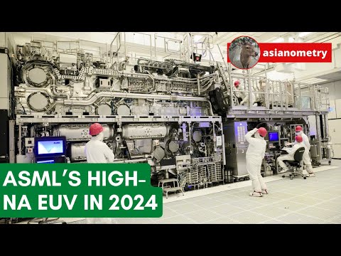
Τα High-NA συστήματα χρησιμοποιούν μεγαλύτερο αριθμητικό άνοιγμα και εξαιρετικά ακριβή οπτική, τοποθέτηση και έλεγχο. Ισχυρισμοί για σταθερότητα πικομέτρων αφορούν συγκεκριμένα υποσυστήματα, όχι μία απλή ακρίβεια όλης της διεργασίας.
Η High-NA EUV μπορεί να βελτιώσει την ανάλυση και να μειώσει την πολλαπλή διαμόρφωση σε ορισμένα κρίσιμα στρώματα. Παραγωγικότητα και κόστος ανά δίσκο εξαρτώνται από ισχύ, έκθεση, αντίσταση, μάσκα, απόδοση και ροή εργοστασίου.

Πηγή: ASML
Η High-NA μπορεί να απλοποιήσει ορισμένες ακολουθίες, αλλά δεν σημαίνει αυτόματα χαμηλότερη κατανάλωση ενέργειας. Τα συστήματα είναι μεγάλα και ενεργοβόρα και η ενέργεια ανά αποδεκτό τσιπ εξαρτάται από ρυθμό και απόδοση.
Η High-NA εξετάζεται για ορισμένα στρώματα στη γενιά 2 nm και κάτω, αλλά οι πελάτες μπορούν να χρησιμοποιούν συμβατική EUV με πολλαπλή διαμόρφωση ή άλλες επιλογές. Η υιοθέτηση θα διαφέρει ανά παραγωγό και στρώμα.

Πηγή: ASML
Η Intel ήταν πρώιμος αποδέκτης High-NA EUV στο Όρεγκον. Η τεχνολογία ακόμη ενσωματώνεται και η εγχάραξη, τα υλικά και άλλες τεχνικές επηρεάζουν επίσης την κλιμάκωση.
«Με την προσθήκη της High-NA EUV, η Intel θα διαθέτει μια ευρεία εργαλειοθήκη λιθογραφίας για δυνατότητες διεργασίας πέρα από την Intel 18A στο δεύτερο μισό της δεκαετίας.»
Mark Phillips — διευθυντής λιθογραφίας, υλικού και λύσεων της Intel Foundry
Η αναφερόμενη τιμή περίπου $400 εκατ. ανά σύστημα ωθεί ορισμένους κατασκευαστές να εξετάζουν καθυστερημένη υιοθέτηση. Η απόφαση εξαρτάται από κόστος, ανάγκη πολλαπλής διαμόρφωσης, ρυθμό και απόδοση.
Η High-NA EUV επαναχρησιμοποιεί μέρη του οικοσυστήματος EUV, αλλά δεν είναι απλό βήμα. Μεγαλύτερη οπτική, αναμορφική απεικόνιση, νέες μάσκες και αντιστάσεις, πεδίο έκθεσης, κόστος και ενσωμάτωση δημιουργούν νέες προκλήσεις.
«Γιατί δώσαμε προτεραιότητα στην κοινή αρχιτεκτονική και την αρθρωτότητα των συστημάτων EUV; Έτσι όλα τα συστήματα αξιοποιούν όσα μάθαμε από 20 χρόνια ανάπτυξης EUV.
Η χρήση δοκιμασμένης τεχνολογίας μειώνει τον κίνδυνο αστοχίας και οι μονάδες διευκολύνουν την εγκατάσταση και ενσωμάτωση στο εργοστάσιο του πελάτη.»
Συμπέρασμα
Οι πολυετείς επενδύσεις της ASML στην ακρίβεια, την ολοκλήρωση συστημάτων και τους προμηθευτές της έδωσαν ηγετική θέση στη λιθογραφία. Παραμένει όμως εξαρτημένη από κρίσιμους προμηθευτές, προϋπολογισμούς πελατών και άδειες εξαγωγής.
Η ASML έχει ουσιαστικά μονοπώλιο στα εμπορικά συστήματα EUV μεγάλης παραγωγής. Η EUV είναι σημαντική για πολλά κρίσιμα στρώματα προηγμένης λογικής και μνήμης, ενώ DUV και άλλα στάδια εξακολουθούν να χρησιμοποιούνται ευρέως.
Δεν είναι δυνατό να γνωρίζουμε πόσο θα διατηρούσε τη θέση της χωρίς τους ελέγχους εξαγωγών. Οι κυρώσεις περιορίζουν την αγορά της και ταυτόχρονα μπορούν να επιταχύνουν επενδύσεις σε ανταγωνιστική κινεζική τεχνολογία.
Οι κινεζικοί παραγωγοί μπορεί να γίνουν ισχυρότεροι ανταγωνιστές, αλλά το τεχνικό χάσμα δεν συνοψίζεται σε μία ονομασία κόμβου. Απόδοση, ρυθμός, οπτική, πηγή, μάσκες, υλικά, μετρολογία και υποστήριξη πρέπει να λειτουργούν μαζί.
Κινεζικοί φορείς επιδιώκουν εγχώρια EUV ενώ η ASML και οι πελάτες εισάγουν High-NA. Δεν υπάρχει επιβεβαιωμένη ημερομηνία εξίσωσης μιας κινεζικής πλατφόρμας με συγκεκριμένη γενιά ASML.
Η ASML έχει σημαντικό τεχνικό και εμπορικό προβάδισμα, αλλά δεν μπορεί να εγγυηθεί κανείς ηγεσία τουλάχιστον δέκα ετών. Ανταγωνισμός, εναλλακτικές διεργασίες, πελάτες, κανόνες εξαγωγών, προμηθευτές και ο κύκλος ημιαγωγών μπορούν να αλλάξουν τις προοπτικές.
Η ASML έχει επίσης ισχυρή θέση σε DUV, υπηρεσίες και ορισμένες λύσεις μετρολογίας. Αυτές διαφοροποιούν τα έσοδα και στηρίζουν την Ε&Α, αλλά εκτίθενται σε ανταγωνισμό, αξιοποίηση πελατών και κύκλους επενδύσεων.
Οι επενδυτές πρέπει να εξετάζουν την τεχνολογική ποιότητα μαζί με την αποτίμηση. Υψηλές προσδοκίες ανάπτυξης μπορούν να προκαλέσουν μεγάλες μεταβολές εάν παραγγελίες, περιθώρια, κανόνες εξαγωγών ή επενδύσεις πελατών αποκλίνουν.
Ιστορικοί δείκτες P/E περίπου 20–54 εξαρτώνται από την ημερομηνία και την περίοδο κερδών. Δεν αποτελούν σταθερή «εύλογη αξία»· χρειάζονται ενημερωμένα στοιχεία για ταμειακές ροές, κύκλο, παραγγελίες, περιθώρια και σενάρια.
Τελευταία Νέα και Αναπτύξεις Μετοχής ASML (ASML)



