Computing
China Master EUV Much Sooner Than Expected
Securities.io maintains rigorous editorial standards and may receive compensation from reviewed links. We are not a registered investment adviser and this is not investment advice. Please view our affiliate disclosure.
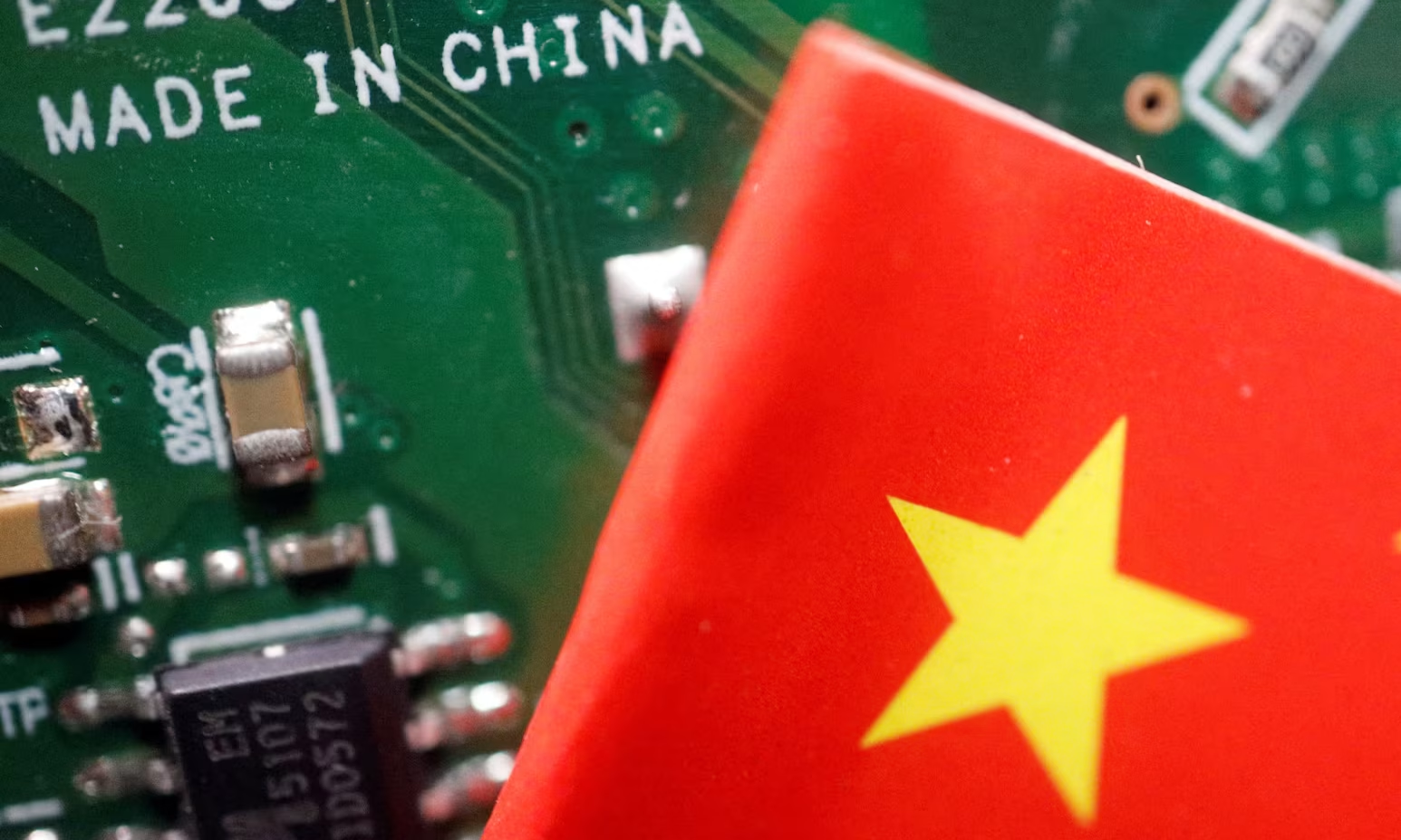
Chinese EUV Prototype Arrives Early
As computing techniques improved, more and more advanced chips were invented. The latest generation of 3nm and 2nm nodes is so small that the normal light wavelength is simply too large to reliably pattern features at this scale.
This is not new, as the industry has long used DUV (Deep UltraViolet) light to perform lithography on silicon wafers. But to reach the nanoscopic scale of the most advanced chip designs, an even shorter-wavelength light source was required.
This light source and lithography method is called EUV (Extreme UltraViolet).

Source: Zeiss
Until now, EUV was the monopoly of the Dutch company ASML (ASML -2.45%), the sole manufacturer of EUV lithography machines in the world.
Back in 2019, TSMC’s 7nm node chips were made with the first EUV process, delivering high-volume customer products to the market.
Control over access to EUV technology has been central to U.S. sanctions on China’s semiconductor industry. As far back as 2018, the United States began pressuring the Netherlands to block ASML from selling EUV machines, related components, and maintenance services.
The idea was that restricting EUV access would slow China’s ability to manufacture leading-edge chips and, alongside limits on exporting advanced AI accelerators, help the U.S. maintain an edge in the AI race.
Except, it now appears China’s push for semiconductor independence has accelerated under pressure, and Reuters reports that China has completed a prototype EUV machine. If development stays on track, it could begin producing chips as soon as 2028, with production ramping from there.
Not only could this complicate Western efforts to constrain China’s access to leading-edge manufacturing, but it may also represent a long-term threat to the Western-centric semiconductor supply chain—arriving years sooner than even many China-optimistic analysts expected.
Summary
China’s unexpected EUV breakthrough challenges ASML’s monopoly, undermines Western sanctions strategy, and signals a long-term shift in global semiconductor power.
China’s unexpected EUV breakthrough challenges ASML’s monopoly, undermines Western sanctions strategy, and signals a long-term shift in global semiconductor power.
How EUV Lithography Actually Works
What makes EUV so unique—and why it remained an ASML monopoly for many years—is that EUV is not just one technology, but the assembly of many feats of ultra-precise engineering into a single integrated system.

The first part is an ultra-powerful CO2 laser rated around 30 kW, making it one of the most powerful pulsed industrial lasers in the world. In ASML’s machines, it is produced by the German company Trumpf.
But it is not this laser that produces EUV light; it is the energy source. To generate EUV, the system overheats tiny droplets of molten tin into plasma, with ASML machines firing roughly 50,000 droplets of tin every second.
The plasma must be driven to extreme temperatures—often cited near 220,000°C (360,000°F)—creating conditions far hotter than the surface of the Sun and pushing industrial engineering to its limits.
The entire process must also occur in a near-perfect vacuum, because air (and most materials) absorb EUV light.

Source: SemiEngineering
And this is still not all. That EUV light now needs to be directed, shaped, and focused with astonishing precision to pattern silicon wafers at the cutting edge—often discussed in terms of transistor densities approaching 100 million transistors per square millimeter for leading nodes.
These curved mirrors, developed by the German optics leader Zeiss, must be manufactured and aligned with accuracy approaching the atomic level.
“If you were to enlarge such an EUV mirror to the size of Germany, the largest unevenness – the Zugspitze, so to speak – would be a whole 0.1 millimeters high.”
This precision is so extreme that the mirrors’ directional accuracy is often described with vivid analogies. For example, if an EUV mirror were used to redirect a beam toward the Moon, it would theoretically be accurate enough to hit an object as small as a ping pong ball on the Moon’s surface.
These optics are also coated with a multilayer stack—often alternating materials like silicon and molybdenum—only a few atoms thick per layer.
“For this, up to 100 layers lie on top of each other here. A single layer would only reflect a good one percent of the light – the loss would be far too great.
The result is a reflectivity that makes up to 70 percent of the light usable.”
Finally, the silicon wafer itself must move and align with extraordinary precision. Sensors measure positioning continuously, and the wafer stage must maintain accuracy while resisting deformation from thermal change and high-speed motion.
So, when taking into consideration all of these steps (and the explanation above is still an oversimplification), it becomes clear why replicating EUV is so difficult: it requires reproducing not only a design, but a vast ecosystem of materials, metrology, controls, optics, vacuum systems, and ultra-clean manufacturing—integrated into one machine.
Why EUV Is So Hard to Replicate
Swipe to scroll →
↔ Horizontal scroll enabled
| Subsystem | Supplier Dominance | Why It’s Difficult |
|---|---|---|
| EUV Light Source (tin plasma) | ASML ecosystem + Trumpf | High-power lasers, droplet timing, plasma stability, debris mitigation |
| Projection Optics | Zeiss near-monopoly | Atomic-level surface perfection, multilayer coatings, yield at scale |
| Vacuum Systems | Multiple specialized suppliers | Ultra-clean vacuum integrity with moving stages and high heat loads |
| Metrology & Sensors | Highly specialized global chain | Real-time nanometer feedback loops; calibration, drift, contamination control |
| Control Software | ASML proprietary | Tight integration across thousands of subsystems; process know-how |
| Wafer Stage & Mechanics | Precision mechatronics leaders | Extreme acceleration without vibration; thermal stability; repeatability at scale |
China’s EUV “Manhattan Project”: Total Semiconductor Mobilization
Total Mobilization
Considering how crucial leading-edge chips are for competition in AI, advanced robotics, and military technology, comparing China’s domestic EUV push to a Manhattan Project is not mere rhetoric—it reflects the scale and urgency of the effort.
First, massive amounts of public and private capital appear to have been poured into the broader semiconductor effort, with at least €37B reportedly mobilized at the beginning of 2025, and likely more through university research, industrial facilities, subsidies to critical suppliers, guaranteed purchases, and state-backed demand for future chips.
And perhaps it should not have come as a complete surprise, with a Huawei EUV-related patent reportedly filed in December 2022.
In parallel, another Chinese company, SMIC, reportedly managed to use older DUV machines to produce 5nm-class chips without EUV—illustrating how strong the incentive has been to “make do” with constrained tools.
Another concept was also explored: generating EUV light via a particle accelerator (synchrotron), a direction discussed as early as 2023 and connected to a scientific publication from 2022.
All these efforts illustrate the colossal importance Chinese institutions and companies have placed on either mastering EUV—or building competitive alternatives without it.
Central to these efforts has been Huawei, the heavily sanctioned Chinese tech giant.
How Talent Acquisition Accelerated China’s EUV Program
Another effort to unlock EUV—more secretive—has reportedly focused on acquiring the experience and human talent that made EUV possible in the first place.
Top engineers, including some who had worked at ASML and later retired, were prime targets for recruitment. Reports also suggest that other current employees of ASML have been approached for recruitment as far back as 2020.
These recruitments were reportedly part of a broader effort to bring top talent into China, with semiconductor experts working abroad being offered signing bonuses and subsidies years ago.
Bending some national rules to make it more convenient for these hired experts also appears to have occurred in isolated cases. For example, some naturalized citizens of other countries were reportedly given Chinese passports and allowed to maintain dual citizenship, despite China officially prohibiting dual citizenship.
The fact that many of these engineers are of Chinese nationality or origin may also have made recruitment easier.
Overall, claims that China “only steals technologies” are often an oversimplification of a fast-growing research and engineering ecosystem. Still, in this specific case, the overlap with ASML trade secrets could be meaningful.
Inside China’s First EUV Lithography Prototype
The result of hiring ex-ASML employees, reverse-engineering EUV parts, and independent development of domestic alternatives appears to have produced a prototype that is significantly larger than ASML’s typical 180-ton, school bus-sized EUV systems—reportedly taking up an entire factory floor.
This could indicate the prototype is either more power-hungry, less compact, less efficient, or simply at an earlier stage of optimization than ASML’s production designs.
Salvaged components from older ASML machines, along with secondhand markets for parts from ASML suppliers, could also have helped assemble a working prototype while domestic manufacturing ramps or quality improves.
A key component that may still be missing—and exceptionally difficult to replicate at comparable performance—is Zeiss optics. This is reportedly one reason the machine cannot yet produce chips at the desired level.
High-NA EUV: The Next Front in the Chip Arms Race
If EUV took ASML decades to develop, the emergence of a Chinese prototype suggests that catching up—at least in basic system demonstration—could happen much faster than many assumed.
This puts pressure on Western semiconductor leaders to push harder into the next generation: High-NA (Numerical Aperture) EUV.
High-NA EUV is already being tested by companies like Intel (INTC +2.2%), and it has been evaluated by Samsung and TSMC. Intel has publicly targeted production volume timelines around 2028, while both TSMC and Samsung appear more cautious, reserving High-NA EUV for future <2nm nodes rather than rushing it into mass deployment.
“The larger the angles from which the optical system picks up light, the finer the details that are displayed. This means that optical EUV systems are becoming larger and larger.”
High-NA systems use even larger optical elements, which may provide a durable edge to ASML via its optics partner Zeiss.

Source: Zeiss
A mirror for High-NA EUV lithography is about twice as large and ten times as heavy as current EUV mirrors—making the total system even larger, heavier, and more complex.
“More than 40,000 parts of the projection optics for High-NA-EUV lithography weigh around twelve tons to ensure high-precision focusing – seven times the volume and weight of the established EUV lithography.”
What Does It Mean For Investors?
In the short term, this likely changes little. China’s EUV machine is reportedly only a prototype, and it remains unclear how much of it relies on repurposed or salvaged ASML parts versus purely China-made components.
However, it is difficult to assume that China will fail indefinitely. With enough specialists, funding, and time, there is no clear reason to believe Chinese institutions cannot eventually replicate much of EUV’s capability—especially as the broader ecosystem of components, materials, and metrology matures.
Skepticism that China cannot replace a specific component, such as Zeiss mirrors, should also be treated cautiously. Similar analyses previously suggested China was 15+ years behind, yet a prototype has now been reported.
In the long term (5–10 years), China could build a parallel semiconductor supply chain that is independent not only at the foundry level, but also at the equipment-manufacturing level.
At first, advanced domestic production would likely prioritize domestic demand, reducing sales to China of advanced chips, manufacturing tools, and supporting components.
Over time, this could pressure the turnover and margins of Western semiconductor equipment makers and suppliers, reducing their ability to reinvest at previous R&D levels.
More concerning for companies like ASML and other equipment makers—and even for foundries—China-made advanced chips could eventually compete directly in external markets, especially across expanding BRICS and SCO (Shanghai Cooperation Organization) commercial networks.
Investor Takeaway
While ASML and TSMC remain dominant near-term, China’s EUV progress introduces long-term competitive pressure that could reshape equipment, foundry, and chip markets.
While ASML and TSMC remain dominant near-term, China’s EUV progress introduces long-term competitive pressure that could reshape equipment, foundry, and chip markets.
Conclusion
The appearance of a Chinese EUV prototype years earlier than many expected is a genuine milestone. It suggests that export controls and sanctions are unlikely to permanently cap technological capability in a sector where the West has long held a structural advantage.
At best, restrictions may delay progress; at worst, they can accelerate it by creating a protected domestic market of roughly 1.5 billion people with strong state support and industrial capacity.
This does not mean China will immediately begin producing leading-edge chips on domestic EUV tools. But it does mean the trajectory toward that goal is now clearer—and likely faster—than many previously assumed.
Overall, it reinforces that China is evolving into a major tech power, not merely the world’s largest manufacturing base.
Some analyses argue China now leads in a large share of advanced scientific domains, which challenges the simplistic narrative that progress occurs only through imitation—even if trade secret disputes and IP conflicts remain a real feature of this competition.
While China’s breakthrough changes the long-term horizon, investors looking for immediate dominance in the semiconductor space must still look to the current market leader.
Semiconductor Company – TSMC
Taiwan Semiconductor Manufacturing Company Limited (TSM -1.85%)
China’s rise as a tech power is strategically significant, but for now, China’s semiconductor manufacturing equipment still appears behind—or only approaching—the most advanced Western systems.
So when it comes to the foundry business, process discipline, yield learning, and operational experience are likely to remain decisive in the decade to come.
Ultimately, semiconductor production is dominated by niche expertise and the ability to mass-produce at scale to reduce cost. No company has mastered that model better than TSMC, the Taiwanese leader in ultra-advanced chip manufacturing.
TSMC primarily produces silicon chips, including the most powerful 3nm and upcoming 2nm-class nodes. And because it manufactures the most advanced (and most expensive) chips, it captures a dominant share of global foundry revenue.

Source: Eric Flaningam
TSMC is also expanding manufacturing capacity in the U.S., notably through major investments in its Arizona fabs.
With High-NA EUV development already underway, TSMC may remain one step ahead of Chinese rivals such as SMIC for years—especially on yield, reliability, and high-volume manufacturing maturity.
And even as it has competed fiercely against Samsung, Intel, and other foundries, TSMC is still positioned to defend its lead against rising China-based competition—at least for the foreseeable future.
Latest TSMC (TSM) Stock News and Developments
Tesla Just Snubbed TSMC — Musk Is Quietly Building A Sovereign Chip Chain
benzinga.com
•
March 18, 2026
The Best AI Stocks to Invest $1,000 in Right Now
fool.com
•
March 18, 2026
TSMC Stock Looks Like a Table-Pounding Gift After That 13% Correction
247wallst.com
•
March 18, 2026
Buy These 3 Semiconductor Stocks Now and Thank Yourself in a Decade
fool.com
•
March 18, 2026
NVDA vs. TSM: Which Semiconductor Powerhouse Offers More Upside?
zacks.com
•
March 18, 2026
TSM Stock: Why Selling Puts Is The Win-Win Play
forbes.com
•
March 18, 2026