Computing
Lace Lithography Replaces EUV Lithography With 10x Smaller Atom Beams

Semiconductor lithography is the most important technology in support of the modern world, forming the basis of manufacturing for chips, memory, AI hardware, and all sorts of electronic components. To this day, the principle of lithography, or more precisely photolithography, is still the same as when it was invented.
A power light source is emitted, concentrated, and direct, so it can etch a pattern on a silicon wafer, creating the transistors and other microscopic components that make modern electronics possible.

Source: Fabricated Knowledge
Of course, this is an oversimplification, as the actual production process involves many other steps of adding and removing materials, removing impurities, stabilizing and packaging the finished products, etc. But still, photolithography is often the most crucial step.
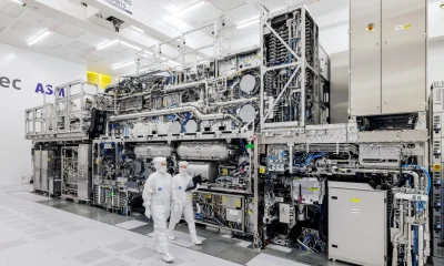
This is perfectly illustrated by the most advanced form of lithography, EUV (Extreme Ultraviolet Lithography) lithography, which utilizes high-power UV rays to engrave as small as possible the silicon wafer. This is a technology almost entirely controlled by one company, the Dutch ASML (ASML ) (see our investment report on the company for more information), although China is actively trying to develop its own independent version of this technology.
“Chips run the world. And making them keeps getting harder. The most advanced lithography machines today cost upwards of €380 million per unit, with the next generation expected to exceed €700 million. They are extraordinarily complex, energy-intensive, and sourced from a single supplier.
Until today, lithography has mostly progressed with an increasingly precise and powerful light source, moving into increasingly energetic wavelengths and complex control systems.
This process might, however, soon reach a limit, as no photolithography can be more precise than the size of the light’s wavelength it uses.

Source: Allresist
This is why teams of researchers around the world are working on alternatives that could create even more refined and powerful computing components, especially in the age of AI demanding ever more powerful computing capacity.
One of these alternatives might be to directly use individual atoms instead of light, an approach advocated by Norwegian company Lace Lithography. The company raised in March 2026 $40M in a series A funding, and is backed by Microsoft.
From Light To Atoms
Moore’s Law Hitting Hard Limits
Photolithography can be extremely precise, engraving the targeted silicon wafer at the nanometer scale. However, for fundamental physics reasons, no light can be more precise than its own wavelengths.
In more technical terms, the main problem is the diffraction limit, where different light beams start interfering with each other and blur the desired pattern.

Source: ResearchGate
So while increasingly powerful EUV light can help, it will hit a hard limit constraint by physics soon, maybe as soon as in 10 years. This would derail Moore’s Law, the empirical trend of the semiconductor industry to double transistor density every two years.
“The result is a manufacturing bottleneck at the heart of the global economy, arriving at exactly the moment AI is driving an unprecedented surge in demand for compute. The industry has known this is coming, but previously nobody has had a credible answer.”
Engraving With Atoms
Diffraction limit is due to the nature of light, which is a wave. But individual atoms are not subject to this limit. Or to be exact, they can behave like waves, like all quantum-scale objects, but with an extremely smaller wavelength than light.
“Atoms behave like waves, but with much shorter wavelengths, enabling significantly finer structures, more powerful chips, and radically lower energy consumption.”
Following this principle, Lace Lithography is developing a method that performs lithography by using a beam of helium atoms instead of light.
The beam Lace Lithography will use to make chips is about the width of a single hydrogen atom, or 0.1 nanometer. In comparison, ASML’s lithography tools use a beam of light that is about 13.5 nanometers, and a human hair is about 100,000 nanometers wide.
Of course, this is not a new idea, as the concept has been considered for decades due to the inherent precision advantages atoms would have over light, especially considering how difficult it is to create and direct light like EUV, which is created by superheating thousands of tiny droplets of tin per second.
But the main issue was the creation of such a mask. Traditional photomasks are made of quartz or glass substrates coated with an opaque film onto which the pattern of the device being manufactured is etched. This film is essentially the template for the chips that will be engraved on the silicon wafer, although it is miniaturized to a much smaller scale during the engraving process.
To create a mask that works with atoms, the mathematics of the problem were considered too complex until now to ever design a mask for atom-beam lithography.
This is now a problem that Lace Lithography claims to have solved.
Lace Lithography
Lace Lithography Overview
The company was launched in 2023 and is looking to be “developing breakthrough chip patterning technology for the next 100 years of chip production”.
It was founded by Bodil Holst, a Danish-Norwegian physicist and an affiliated professor in the Department of Physics and Technology at the University of Bergen in Norway, with Adria Salvador Palau, her former PhD student.
The company has facilities in Norway, Spain, and the Netherlands, with its headquarters in Bergen, Norway.
In order to solve the problem of creating masks for beam lithography, the team leveraged AI to figure out the previously unsolved mathematics. This illustrates how AI might not just change how we perform some tasks, but unlock entirely new possibilities in hard sciences and engineering.
“The remaining hard problem was mask design: the mathematics involved were considered effectively intractable. Lace solved it with a proprietary AI-driven algorithm that accelerates the computation by over 15 orders of magnitude. This is not an incremental improvement. It is a category shift.”
In theory, this technology could allow for engraving 10x smaller than even the most advanced light-based lithography.
The company presented the science behind its achievement at the Advanced Lithography + Patterning scientific conference in San Jose, California, held by SPIE.
In the abstract of this presentation, it is explained that the “fundamental advantage of using metastable atoms for lithography is that the patterning resolution is decoupled from the patterning energy.” This means that the atom beam can be more or less powerful on demand, contrary to light, which needs increasingly small wavelengths for higher energy levels.
“We demonstrate two different exposure modes: proximity and diffraction. For proximity, we present patterns of holes down to 50 nm CD at a half pitch of 100 nm. For diffraction, we present a regular line pattern with a half pitch of 50 nm.”
The mask technology can be scaled to the current size of silicon wafer used by the industry, and could even be extended further.
“Furthermore, we present the first AI-based Inverse Lithography Technology (ILT) diffraction mask designs for atoms. We show that the mask designs can produce arbitrary patterns with a theoretical resolution limit down to the atomic spacing of silicon. The mask design simulations can be scaled to the current full field size and beyond.”
Besides Atomico, the company has received funding from Microsoft’s (MSFT ) venture arm M12, Linse Capital, the Spanish Society for Technological Transformation, and Nysnø. Lace Lithography’s total valuation has not been disclosed.
Getting Ready For Commercialization
Of course, there is time between the unveiling of a scientific breakthrough and a prototype, and actual large-scale utilization of a technology.
However, Lace Lithography is likely going to be, relatively speaking, easy to integrate into semiconductor foundries. It replaces the EUV light source with the helium beam and the traditional photomask with the beam mask design with AI. So there is no need to redesign the assembly line or most of the supply chain already serving the semiconductor manufacturing industry.
Already armed with a prototype, the company is looking to have a test for its first commercial-grade tool in a pilot chip fabrication plant (“fab”) around 2029
Investing In Atom-Beam Lithography
Microsoft
(MSFT )
This technology is still extremely new, and will likely not see any actual commercial chip produced with it before 2030, and no mass deployment before 2035 at best.
However, this could be a game-changer in the long term, removing the dominant player, ASML, entirely from its monopoly position in lithography. As ASML is currently valued at $450B, even a small participation in Lace Lithography could pay off massively in the future.
As most investors are not able to directly invest in an early startup like this company, exposure to Microsoft’s stock is probably the second-best option.
The operating system and software giant is also making plenty of bets on innovative technology, with AI, especially AI applied to B2B uses and scientific research, a key focus of the company. In the past decade, Microsoft has also become a company pushing the limit of some of the most promising technologies and taking more risks than in past decades:
- Quantum computing chips, inventing an entire new state of matter (topoconductors).
- Nuclear fusion, with a reactor to be delivered to Microsoft by Helion Energy as soon as 2028.
- Moving early in restarting nuclear power plants to power AI data centers.
- Scientific AIsfor material sciences, chemistry, and biology.
- B2B and PC-based AI(Copilot)
In addition to these activities, the company is a leader in operating software, B2B software (Office), B2B social network (LinkedIn), video game development, gaming console (XBox), cloud computing, and AI development.
This means that while atom-beam lithography is likely not going to add by itself another trillion to Microsoft’s already massive market cap, this is one of the very promising fields in which the company has invested early on. So the stock could provide upside from disruptive “moonshot” innovation while also providing exposure to the company’s more stable and predictable core activities.
(You can read more about Microsoft’s business as a whole in our investment report dedicated to the company.)
Latest Microsoft (MSFT) Stock News and Developments